Upload BOM & Gerber
-
Mobile: +86 13312967631
-
Email: sales@sugaintl.com

Flex & Rigid-Flex PCB Assembly Services
China Flex and Rigid-Flex PCB Assembly Supplier with Flex-Zone Control from Fabrication Through Assembly
Align materials, bend zones, carrier support, SMT, controlled reflow, inspection and functional validation before prototype settings move into production.
SUGA supports flex circuits from 1–6 routine layers and 7–10 extended layers. Routine rigid-flex constructions support up to 26 total / 10 flex layers, while extended constructions reach up to 30 total / 18 flex layers.
0.1 mm Laser Vias · 3+n+3 HDI
X-Ray · Microsection · Flex-Cycle Test
Flex PCB vs. Rigid-Flex PCB Assembly
A flex PCB uses a flexible polyimide material to carry conductors within a bending environment. A rigid-flex PCB has both flexible and rigid sections, providing a direct connection between them. When assembling devices, consider using flexible PCBs when there is a need for the PCB to be flexed and routed through narrow areas or continuously over a defined bend radius, and select rigid-flex when there are mechanical requirements for the assembly—for instance, if the components must be firmly supported—and the integration of multiple components into a single assembly with fewer interconnections.
The initial decision of whether to use a rigid or flex PCB should be made based on movement rather than the designation of the PCB. A fixed assembly may require a rigid PCB for basic function, while a flex-to-install circuit is flexed during installation and remains mostly stationary through use. In contrast, a dynamic flex circuit would be performance-tested to ensure continued movement over time. These two flex circuit configurations will have different stackups and validation plans.
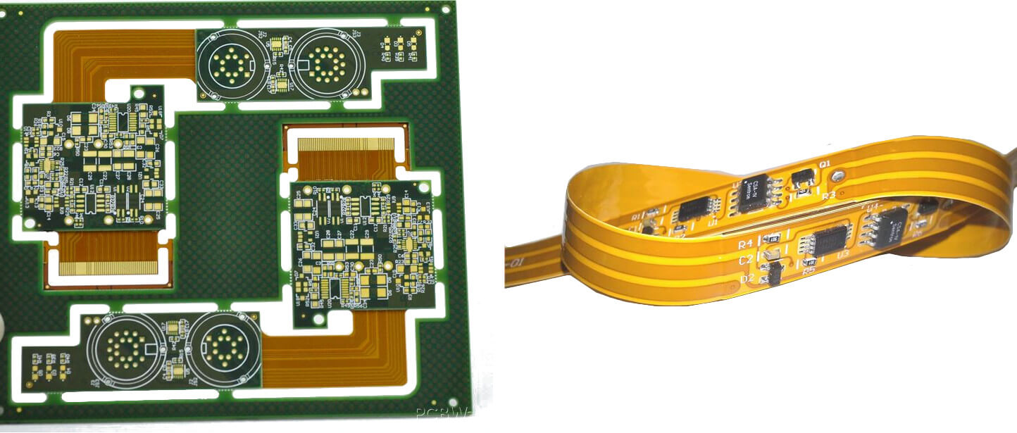
| Board structure | Bend behavior | Component mounting | Interconnection | Main assembly concern | Typical use |
|---|---|---|---|---|---|
| Rigid PCB | No designed bend | Components are supported across the board | Connectors or cables link separated boards | Planar support through standard printing, placement, and reflow | Flat control, power, or interface boards |
| Flex PCB | Static fold, flex-to-install, or defined dynamic bend | Component zones need local carrier or stiffener support | Can replace cables and simple interconnects | Keep bend zones flat during SMT and free from local loading | Thin routing through narrow or moving spaces |
| Rigid-Flex PCB | Rigid areas joined by controlled flex sections | Components remain on rigid zones | Reduces board-to-board connectors and jumpers | Protect rigid-to-flex transitions through assembly and handling | Compact 3D assemblies with stable component mounting |
Continuous-Motion Flex Assembly
Continuous-motion flex assembly requires additional consideration of how the finished stackup must perform.
When designing the flex-to-install assembly, consideration must be given to how the assembly process will provide support for the circuit during bending and when it is put into its final position within the product.
The component zones of the assembly where components will be installed require local support at the component locations, even though the flexible area must be free to move upon installation and thereafter. The printed circuit panel must lie flat on its carrier during assembly, and additional support may be required for the connector or component after assembly.
The edges of these support areas should never extend into the active bend areas of the assembly.
When Should Rigid-Flex Replace Connectors?
Rigid-flex assemblies are preferred when rigid component areas occupy different planes and flexible connectivity can bridge these connections within the assembly. In these cases, rigid-flex provides a means of reducing connectors, jumpers, and cable assembly steps while still maintaining all loads associated with the components in the rigid locations.
The architecture takes advantage of the rigidity of the rigid sections for packages, connectors, or shielding, while the flex section is used to carry signals or power through a controlled fold. The end result may allow for less overall volume in a compact enclosure; however, the transition geometry, stackup, carrier strategy, and inspection requirements must be validated prior to production release to ensure that they meet product requirements.
The final selection will be determined by whether the design requires integrated rigid support or just a thin flexible interconnect.
Design Rules That Prevent Flex Damage
Most flex damage is caused by factors prior to assembly. The layout is the basis for defining the bend zone, trace path, component location, support edge, and rigid-to-flex transition point; therefore, if a layout has features that concentrate strain, even an efficient SMT process will most likely be unsuccessful at restoring the lost mechanical margin.
Before finalizing the stackup for your flex PCB, please review the checklist to ensure compliance with the design rules.
- Create the finished-stackup bend rule based on the construction and the intended usage instead of one universal multiplier.
- Do not place components or solder joints in either active bend or transition stress zones.
- Match the material, thickness, adhesive, outline, and load path of the stiffener to the component or connector load.
- Route traces in the bend area smoothly; avoid sharp corners and abrupt width changes.
- Avoid routing vias, pads, copper discontinuities, or rigid edges in the high-strain transition areas.
- For each failed checklist item, identify the probable failure mechanism and the required corrective action.
How Is Bend Radius Set?
The bend radius of a flex PCB depends on the finished construction, not the polyimide material itself. The number of layers, the type and thickness of copper, the adhesive or adhesiveless construction, the coverlay, the direction of the bend, and whether the application is static or dynamic all affect the allowable bend of a circuit. Likewise, a given circuit can experience different bending behavior with the same outline based on how these factors change.
The design of the circuit should specify the radius, angle, bend axis, and moving length under the bend condition. The loading, environment, and failure threshold relate to the flex-cycle validation of the circuit. One rule for the flex PCB bend radius cannot account for all single-layer, multilayer, static, and moving constructions.
Where Should Components and Stiffeners Go?
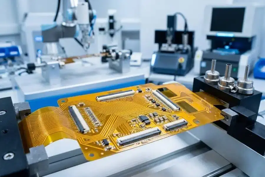
Do not place soldered components or solder joints in the active bend or at the rigid-to-flex transition. Adding a mass to this area creates stiffness within a flexible structure, causing movement to transfer strain to the solder joint, copper pad, or trace instead of spreading it over a controlled length of flexible construction.
If you must add a connector or heavy component to a flex construction, make sure to add support with a properly rated FR-4, PI, metal, or adhesive-backed stiffener. The type and amount of support must match the insertion force, component mass, local coplanarity, adhesive outline, and final load path. Be careful with the stiffener edge location, as incorrectly positioned edges simply create another stress concentration.
Curved Traces Across Bend Areas
Traces that will cross the bend should have smooth geometry and maintain a constant path with respect to the axis of the bend. Sharp corners, abrupt changes in trace widths, and local discontinuities in copper add localized stress concentrations at those points. Curved routing provides a gradual change of direction for the trace; however, the curve does not compensate for an undersized bend radius or improper copper foil construction within the flex circuit.
Keep the same strategy for the routing of traces across the flex area. All return paths, impedance structures, and local balances of copper are still important, and as such, the electrical and mechanical requirements of the flex PCB must be addressed in the same stackup.
Where Should Vias Sit Near Flex Transitions?
Vias and pads add local stiffness to the flex circuit and decrease the copper length that can effectively absorb movement. Avoid locating vias and pads in the high-strain area of the transition from rigidity to flexibility. Avoid placing a rigid edge, via field, and bend start at the same location. The transition from flex to rigidity needs to change in local stiffness gradually.
Annular ring, hole shape and size, plating, pad geometry, registration, and product class all determine the final design for the vias. Do not apply a standard distance to all designs; define the geometry using the finished stackup and mechanical model. Measure the geometry during fabrication.
Materials and Stackups That Survive Reflow
The material set determines where the circuit can bend, where components can be supported, and how the assembly responds to heat. The table gives the primary role of each material.
| Material or structure | Primary role | Assembly impact |
|---|---|---|
| Rolled Annealed (RA) copper | Provides a higher flex-fatigue margin in repeated-bend regions | Bend duty still depends on copper thickness, trace direction, stackup, radius, and cycle conditions |
| Electro-Deposited (ED) copper | Supports fine definition, static flex-to-install regions, or rigid-zone construction | Dynamic use is validated on the finished construction |
| Polyimide | Forms the flexible dielectric in bend zones | Film thickness, moisture condition, adhesive system, and copper affect reflow and bend response |
| FR-4 or specialty rigid laminate | Supports components, connectors, and routing in rigid zones | Adds stiffness and thermal mass that must be reflected in carrier and reflow settings |
| Coverlay | Protects flex conductors and defines exposed pads | Opening registration and edge location affect soldering and transition strain |
| Bondply or bonding film | Joins flex layers or rigid-to-flex regions | Controls dielectric thickness, resin flow, registration, and Z-axis behavior |
| Low-flow prepreg | Bonds rigid regions while limiting resin flow into flex openings | Cure and flow affect lamination quality and flex-window cleanliness |
| Adhesiveless polyimide copper-clad | Removes the conventional adhesive layer between copper and polyimide | Can reduce buildup and Z-axis expansion, although thick copper or PI still increases bend stiffness |
| Stiffener and PSA | Supports connectors, components, and local loading areas | Edge position, adhesive thickness, peel strength, temperature resistance, and cleanliness affect assembly reliability |

Polyimide vs. FR-4
While polyimide materials have some resistance to bending and assembly heat, the combination of a specific film with the proper adhesive and copper construction is needed to ensure success. FR-4 materials do not provide a designed bend allowance but do provide support for components, routing, connectors, and local mechanical loads within rigid zones.
The most noticeable differences in the assembly of mixed-material systems will occur during the reflow process. The thermal mass and expansion of mixed materials will vary. The reflow profile as well as the carrier must consider these variables for both the thin flex regions and the thicker rigid regions. The assembly must remain supported while it is hot as well as during controlled cooling.
Coverlay and Interlayer Bonding
The role of the coverlay material ends once it meets the pad opening, while the bondply or bonding film acts as a separate material that joins the flex layers internally and bonds the flex and rigid areas of the assembly. The use of bondply as coverlay can result in misinterpretation of thickness and openings during fabrication due to mixing the two terms. The low-flow prepreg that adheres to rigid regions will minimize the possibility of resin flowing into flex openings.
Bonding systems based on epoxy, acrylic, or polyimide will exhibit different cured Tg values, moisture-response properties, peel strengths, curing conditions, and reflow behaviors. The application of PSA for stiffening support, mounting support, or non-electrically active support zones is only possible where the parameters of temperature, thickness, peel, and cleanliness allow it.
Which Copper Suits Dynamic Bending?
When designing for repeated bending, RA copper will typically be the preferred choice due to its ability to provide an improved flex-fatigue margin in a suitable construction. Conversely, ED copper will generally fit static flex-to-install regions, rigid zones, or layouts where fine definition is considered more critical.
Adhesive vs. Adhesiveless Flex
While adhesive-based flex can provide the benefits of bonding and peel strength, the use of an adhesive also results in greater thickness and creates an additional interface layer. The absence of an adhesive layer between copper and polyimide in adhesiveless construction can reduce material buildup and Z-axis expansion and can also be a better option for applications where dynamic flex is present. The trade-offs associated with using adhesiveless material are dependent upon how the laminate, copper, coverlay, support, reflow exposure, and bend duty are matched. Thicker copper or PI will generally limit the bend performance of adhesiveless circuits, while an adhesive-based construction will support bending when the material system matches the performance requirement.
Flex and Rigid-Flex Assembly Process
The assembly of flex and rigid-flex circuits is staged to provide support to the circuit during soldering and handling in six stages:
- Verify packaging, material condition, cleanliness, moisture-sensitive requirements, and the initial flatness of the PCB at the time of receipt in the assembly facility.
- Define datum points for carrier support at local support areas and determine load repeatability and the condition of printable surfaces prior to loading.
- Control stencil design, paste release, fiducials, component placement force, and component loading.
- Match the reflow profile with the material system and maintain panel support while hot and during controlled cooling.
- Provide local support for through-hole connectors and any mechanical or mixed-technology soldering used.
- Clean and separate panel parts without causing creasing, tensile loading, edge tears, or latent conductor damage.
Preparing Flex Circuits for Assembly
Incoming inspection will determine whether the boards are in a stable state for heat and handling. During this process, the packaging condition, the condition of materials inside the packaging, contamination, and initial flatness of the PCB will provide information regarding possible instability or risk. Preconditioning by baking does not occur automatically; it will depend upon the storage history of both the PCB and the material prior to arrival at the assembly line.
Then the carrier takes the thin panel and makes it a repeatable assembly base. Datums are used to control registration, and local inserts support component zones, while the loading method prevents the flex from stretching or buckling. The support must follow the shape of the flex and component zones as well as the outer outline of the panel.

SMT Processing on Flex Circuits
The transfer of paste depends on having a flat, clean, stable surface for registration. The design of the stencil, aperture release, fiducials, placement force, and component loading must account for local flex deformation in the component zone. Excessive placement force may cause unsupported areas of the flex to move out of their intended plane.
The reflow profile creates another type of load. The profile must be consistent with the solder paste used, components, flex materials, rigid laminates, and adhesives in the assembly. The assembly must be supported while hot and throughout the cooling cycle to avoid warping, delamination, joint stress, and handling marks at the flex transition.
Through-Hole and Mixed Assembly
Connectors and mechanical parts will introduce insertion force, soldering heat, and weight after SMT processing. Local support will hold the component zones while selective, manual, or mixed-technology soldering is being completed. The method used will depend on the component geometry and how the component will be exposed to heat, rather than following a single universal process.
An operator should not grip or lever against an unsupported section of flex. Connector seating, pin alignment, and access for soldering must work with the stiffener and carrier design established earlier.
Protecting Flex After Reflow
Cleaning must remove residues from the manufacturing process without attacking the materials in the assembly or creating a liquid trap around stiffener edges and transitions. After inspection, the depaneling method should follow the panel outline, material, tabs, and flex-zone location. Separate the assembly without creating excess stretching or sharp bends.
The method of final packaging of the assembly is critical. An assembly that is manufactured correctly can still leave the manufacturing facility with a crease or edge load. The flexible zone of the product should be held in the prescribed bend shape only when specified in the product drawing. Otherwise, protect the flex zone from excessive folds, tensile loads, contamination, and contact with sharp hardware edges.
Flex and Rigid-Flex Defect Detection
Areas of risk include the bend zone, rigid-to-flex transition, supported SMT areas, rigid component zones, and the internal rigid-flex structure of the assembly.
| Board area | Defect or signal | Primary verification | Containment or engineering response |
|---|---|---|---|
| Flex bend zone | Crease, edge tear, conductor crack, or intermittent open | Visual and dimensional inspection; continuity or resistance monitoring under a defined bend | Segregate affected units and correct handling, depaneling, bend radius, or cycle conditions |
| Rigid-to-flex transition | Stress concentration, copper crack, or delamination | Visual inspection, microsection, and electrical test; X-ray where the structure is visible | Hold the affected lot and compare transition geometry, lamination, reflow, and handling conditions |
| Coverlay and pad opening | Opening misregistration, pad coverage, or lifted edge | AOI, visual inspection, and dimensional measurement | Correct opening geometry or registration and re-inspect affected assemblies |
| Stiffener or connector zone | Stiffener shift, adhesive void, pad lifting, or local deformation | Visual and dimensional inspection; connector seating or functional check | Correct stiffener outline, adhesive, local support, or insertion loading |
| Carrier-supported SMT area | Paste variation, placement shift, or local warpage | SPI, AOI, visual inspection, and flatness measurement | Correct carrier support, loading repeatability, stencil registration, placement, or thermal profile |
| Rigid component zone | Hidden BGA/QFN/LGA joint anomaly | X-ray with electrical or functional testing; cross-section when root-cause confirmation is needed | Isolate affected assemblies and compare paste transfer, package, and reflow conditions before disposition |
| Internal rigid-flex structure | Microvia, via-barrel, registration, or internal delamination concern | Microsection and electrical test; X-ray where radiographic contrast is available | Hold the affected lot and compare material, drilling, plating, lamination, and reflow history |
| Dynamic flex circuit | Resistance drift or fractured trace during movement | Continuity monitoring, resistance trend, and failure-location analysis under the defined motion | Reconfirm the defined bend and cycle-validation parameters against the failed unit before disposition |
Surface Process Inspection
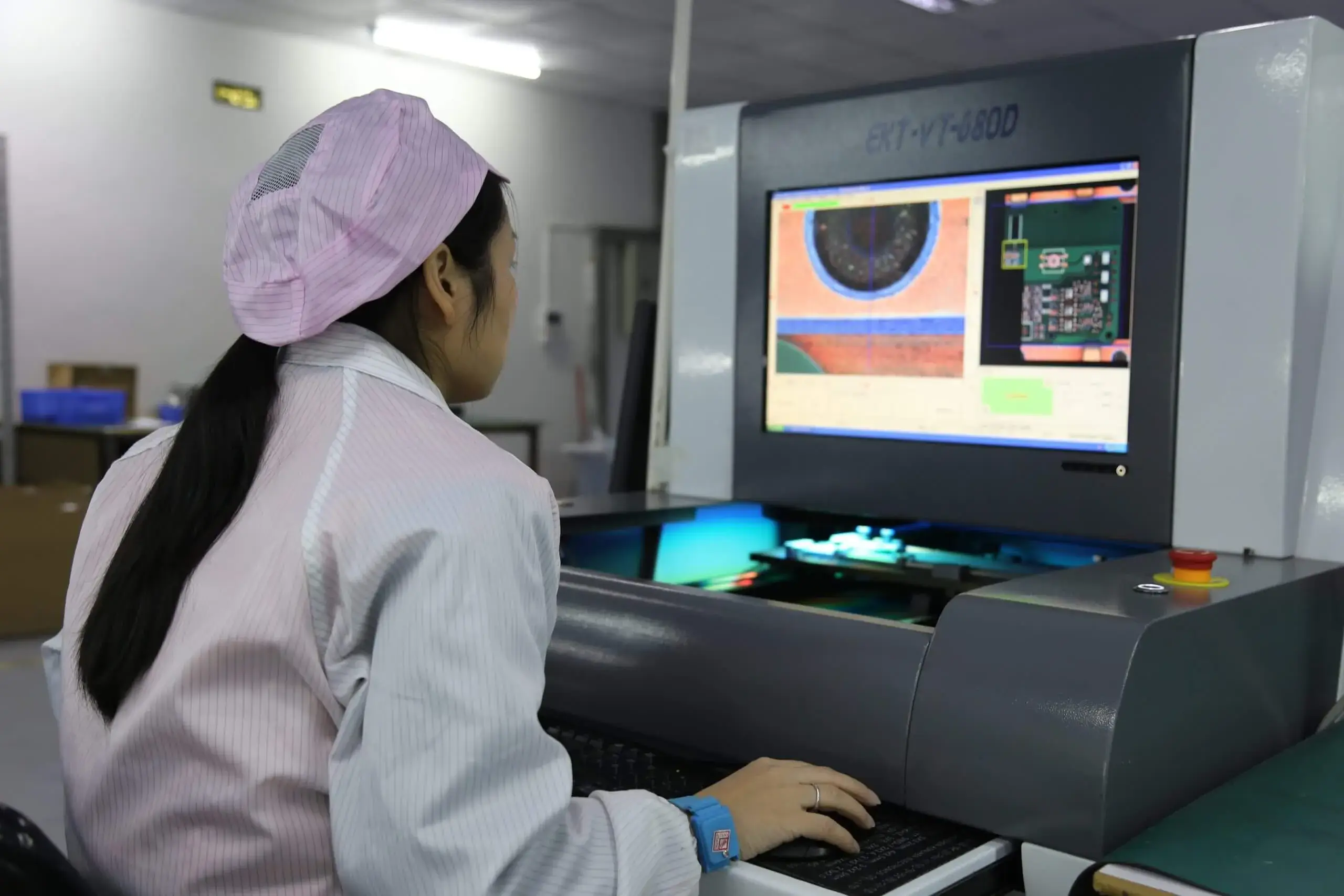
SPI and AOI results on flex and rigid-flex SMT are interpreted against carrier support and local planarity. Repeated paste deviation or component misregistration in one flex area may indicate a support, loading, or stencil-registration issue. Therefore, visual and dimensional inspections will also be performed for coverlay openings, stiffener locations, transition creases, and edge damage.
Hidden-Joint and Internal-Structure Inspection
X-ray is used to inspect hidden joints in rigid component areas. Microsection inspection is used to identify problems in rigid-to-flex transitions, microvias, via barrels, registration, and delamination that cannot be identified through surface inspection methods.
Electrical and Flex-Cycle Validation
E-test is performed on the bare board to check for opens and shorts prior to the installation of components. AET checks the electrical continuity of the completed assembly against a defined fixture or program. FCT checks the functionality of the product. Each of these three tests provides answers to different questions about the assembly and operation of the product.
Provide the following information for documentation: bend radius, angle, frequency, load, environment, powered or unpowered state, target cycle count, monitoring method, and failure threshold. Once the above information is documented, trend analysis and failure-location analysis of continuity results from the testing will be useful for connecting an intermittent or fractured trace with the specific movement described. Without those definitions, a cycle count cannot describe service life.
Flex and Rigid-Flex Manufacturing Ranges
SUGA separates routine ranges from extended engineering ranges and verifies that all structures meet the applicable material, geometrical, and reliability specifications.
| Engineering capability | Routine range | Extended range | Verification |
|---|---|---|---|
| Flex base materials | Adhesive: Shengyi SF302, PI 0.5/1/2 mil with Cu 0.5/1 oz; SF305, PI 0.5/1/2 mil with Cu 0.33/0.5/1 oz. Adhesiveless: Panasonic R-F775/R-F777, PI 1/2/3 mil with Cu 0.5/1 oz; Xinyang/Taihong, PI 1/2 mil with Cu 0.33/0.5/1 oz | Selected 2 oz Cu; PI to 4 mil; additional adhesive or adhesiveless constructions by material code, Cu type, bend duty, and supply | Material certificate, stackup, thickness/dimensions, lot traceability, flex qualification |
| Coverlay, bonding, and support | SF305C 0515/0525/1025/1035/2030; Dongyi adhesive 25/40 μm; SF302B 25/40 μm; MHK PI stiffener 3/5/7/9 mil; 3M 9077/9460/6677/9458; EM-37B(L); PSR-9000 FLX501 | Alternative coverlay, bondply, PSA, steel stiffener, low-flow prepreg, and flexible solder mask by thermal, peel, thickness, registration, and reflow conditions | Certificate, drawing/stackup, dimensions, peel/cure data, qualification |
| Rigid-region laminates | ITEQ IT-180A; Shengyi S1141 and S1000-2M | Arlon 85N, Rogers RO4000, Nelco N4000-13, Ventec VT-901, or equivalent specialty systems | Certificate, stackup, coupon/TDR, microsection, dimensions |
| Flex layers and thickness | 1–6 flex layers; 0.05–0.50 mm finished flex without stiffener | 7–10 flex layers; 0.50–0.80 mm under defined stackup and bend duty | Thickness, dimensions, E-test, flex validation |
| Rigid-flex layers and thickness | Up to 26 total / 10 flex layers; 0.30–5.00 mm finished thickness | Up to 30 total / 18 flex layers with controlled lamination, registration, materials, and HDI structure | Stackup/DFM, registration, microsection, E-test, flatness |
| Finished product size | Flex: 5×10 mm bridgeless or 10×10 mm with bridge to 9×14 in | Flex: 4×8 mm bridgeless or 8×8 mm with bridge to 9×23 in when PI ≥1 mil; rigid-flex: 10×15 mm to 16×29 in | CAM, dimensions, tooling trial, flatness |
| Fine geometry | Finger tolerance ±0.10 mm; finger-to-edge 8 mil; pad spacing 4 mil; trace 3.5 mil, local 3.2 mil; solder-mask dam 4/8 mil below 2 oz and 6/8 mil at 2–4 oz | Finger tolerance ±0.05 mm; finger-to-edge 6 mil; pad spacing 3 mil; trace 3.0 mil, local 2.75 mil under controlled Cu, finish, imaging, and registration | AOI, dimensions, coupon, solder-mask inspection |
| Holes and via structures | Laser hole 0.10 mm; finished flex PTH 0.30 mm; NPTH ±2 mil | Mechanical-via aspect ratio to 12:1; laser aspect ratio to 0.8:1; directional NPTH +0/−2 mil or +2/−0 mil | Hole measurement, AOI, microsection, registration, E-test |
| Controlled impedance | Single-ended/differential: ±5 Ω at ≤50 Ω; ±10% above 50 Ω | Single-ended: ±3 Ω at ≤50 Ω and ±8% above; differential: ±4 Ω at ≤50 Ω and ±8% above | Stackup/field solver, coupon, TDR to IPC-TM-650 2.5.5.7 or equivalent |
| HDI buildup | 2+n+2; buried vias ≤0.40 mm | 3+n+3; blind/buried, stacked, or staggered microvias under defined reliability targets | Microsection, registration, E-test, reliability data |
| Surface finish | OSP, leaded/lead-free HASL, ENIG, hard gold, immersion silver | ENEPIG, soft gold, immersion tin, selective finishes | Finish thickness, solderability/contact inspection; IPC-4552B or IPC-4556 as applicable |
| Bow and twist | Set by panel, assembly, and acceptance conditions | 0.75% symmetrical; 2% asymmetrical; 1.5% tighter custom asymmetrical | IPC-TM-650 2.4.22 or equivalent; placement and solder-joint inspection |
Signal control and HDI buildup determine how these ranges apply to a specific stackup.
How Do HDI Structures Affect Signal Control?
Controlled impedance requires a defined target impedance and physical structure. The following parameters will affect the TDR result: material Dk, dielectric thickness, copper, trace geometry, reference-plane geometry, copper treatment, and lamination.
Using a 2+n+2 or 3+n+3 buildup increases sensitivity to lamination and registration because of the additional sequences.
For blind, buried, stacked, or staggered microvias, the inspection and reliability evidence must match the actual via architecture.

What Drives Flex and Rigid-Flex Assembly Cost?
| Cost driver | Cost effect | Why it changes flex or rigid-flex cost | Design or ordering implication |
|---|---|---|---|
| Flex-layer count and rigid-flex allocation | Usually rises with added layers and rigid sections | More materials, lamination, registration, drilling, and inspection increase process exposure | Use only the layers and rigid zones required for routing, support, shielding, and mechanics |
| Sequential lamination and HDI buildup | Rises with additional buildup cycles and tighter registration | Blind, buried, stacked, or staggered vias add process steps and internal-structure inspection | Compare 2+n+2 or 3+n+3 buildup with the routing density and product envelope |
| Flex materials, coverlay, and stiffeners | Rises with specialty laminates and local support features | Material combinations, coverlay openings, bonding films, stiffeners, and selective finishes add setup and handling requirements | Define the material system and support areas before tooling and process planning |
| Dedicated carrier and assembly tooling | Adds one-time engineering and maintenance cost | Thin flex needs repeatable flatness, datums, local support, loading, and unloading | Stable panel geometry allows tooling cost and setup effort to be reused |
| Inspection and flex validation | Rises with hidden-joint, internal-structure, or movement coverage | X-ray, microsection, functional testing, and defined flex-cycle testing require programs, fixtures, time, and records | Match coverage to package visibility, bend duty, acceptance class, and failure consequence |
| Prototype vs. repeat production | NRE is concentrated in prototypes and allocated across repeat builds | Carrier, stencil, profiles, programs, and first-article work are front-loaded | Preserve the production baseline so repeat orders do not recreate setup |
NRE work is typically performed on the first article; a geometry change, a material change, or a process change large enough to require requalification resets the baseline and therefore incurs the cost of another first article if the design or associated configurations change between baseline production and repeat orders.
Flex and Rigid-Flex Applications
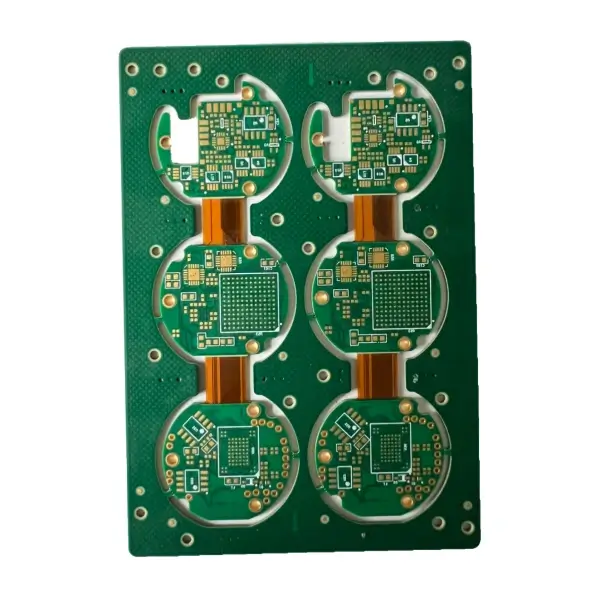
Rigid-flex PCB applications are best where the product requires both supported component zones and a thin interconnect that is routed through constrained space. Flex works best when the interconnect itself is required to carry a static or specific moving bend. In addition to the configuration of rigid or flex circuits, the end-product design will dictate the physical structure. Loading, assembly access, and validation will also determine the structure.
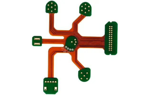
Medical Device PCB
The design of implantable and wearable medical devices includes the routing of sensors or displays within sealed, biocompatible enclosures. A typical structure of a flex PCB for medical devices consists of 2 layers, 0.10 mm polyimide, and a 3 mil solder-mask dam. In contrast, reusable external instrumentation adds repeated autoclave cycles, thereby creating a greater risk of adhesive-based coverlay softening compared with adhesiveless flex construction. Electrical and functional validation follows IEC 60601, while sterilization and biocompatibility must be validated separately under the applicable standard.

Automotive Electronics PCB
Automotive electronics may include door control systems, ADAS sensors, cameras, and actuators. These assemblies combine tight routing with thermal cycling and mechanical vibration. An example of a validated automotive electronics assembly configuration consists of 4 layers, 4 mil traces / 3 mil spacing, an approximately 0.2 mm BGA pad diameter, a blind via, and a custom signal/power/flex stackup. The assembly process requires rigid-zone BGA support and local fixturing. Board-level evidence includes SPI/AOI, X-ray, and electrical or functional records.

Aerospace Avionics PCB
Avionics, navigation, satellite, and communication assemblies are manufactured using rigid-flex to reduce reliance on connectors and route between planes without creating loose cable loops. Altitude-driven pressure and temperature cycling can loosen stiffener adhesive at rigid-to-flex transitions faster than ground-based duty; therefore, the validation plan covers hidden joints, internal structures, continuity, function, vibration according to DO-160, and the applicable aerospace requirements.
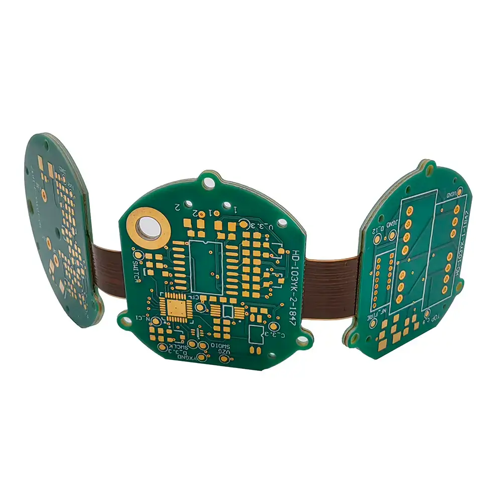
Wearable and IoT PCB
Wearable devices such as GPS trackers and compact sensors frequently use folding circuits assembled into compact enclosures. An example GPS tracker configuration uses 2 layers, a 0.5 mm rigid region, a 0.12 mm flex region, a 4 mil solder-mask dam, PI adhesive or adhesiveless construction, and typical 1 oz copper. Assembly controls include positioning, transition support, and antenna-area isolation. Continuity, visual, and functional checks apply, and any repeated bend follows the flex-cycle validation parameters.
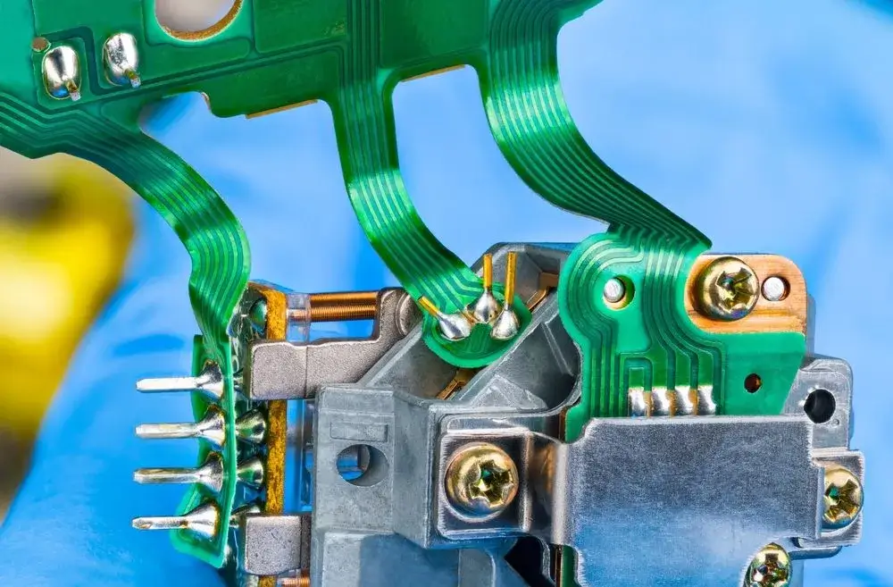
Industrial Motion and Scanner PCB
Robotics, motion systems, and scanners may expose an interconnect to repeated handling or controlled travel. A single-layer scanner flex uses 0.13 mm thickness, 1 oz RA copper with adhesive or 35 μm copper, 0.10 mm trace width / 0.095 mm spacing, and a 0.5 mm FR-4 stiffener. Terminal-zone positioning and carrier flatness help protect the thin circuit. Visual/AOI, dimensional, and continuity checks will be conducted for this assembly.
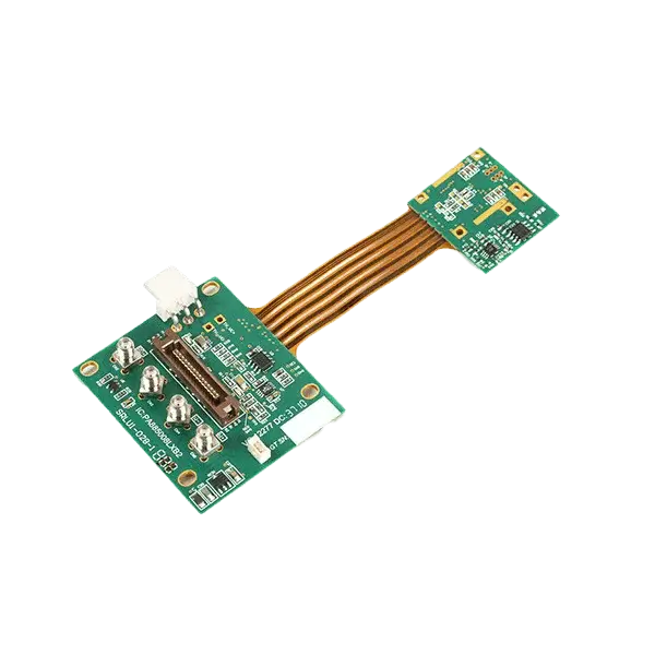
Consumer Display and Mobile PCB
LCD connectors, cameras, display modules, and mobile mainboards require precise alignment within a thin enclosure. A typical LCD connector configuration uses 0.15 mm thickness, ±0.03 mm positional accuracy, front and back 0.15 mm steel stiffeners, 0.06 mm trace width / 0.09 mm spacing, and ENIG controlled by the specification and IPC-4552B. A second configuration consists of a 10-layer, 1.5 mm rigid-flex mainboard with 3 mil traces / 4 mil spacing, a 5 mil solder-mask dam, PI plus RA flex, high-Tg FR-4, and optional blind or buried vias. SPI/AOI, X-ray, and electrical testing or FCT depend on package visibility.

Telecom RF Module PCB
Routers, modems, and RF modules commonly use rigid-flex construction because it allows controlled interconnects to be routed through three-dimensional packaging. A typical RF-flex stackup combines a Rogers or PTFE rigid section with polyimide flex zones to maintain single-ended impedance within ±3–5 Ω; therefore, folds near the RF section should be designed so that they do not produce dielectric changes that increase insertion loss.
What Shows Repeatable Flex Assembly?
To achieve repeatability as a manufacturer, you need a documented, traceable production baseline that directly correlates the materials used, tools used, production programs, inspection results, and completed assemblies.
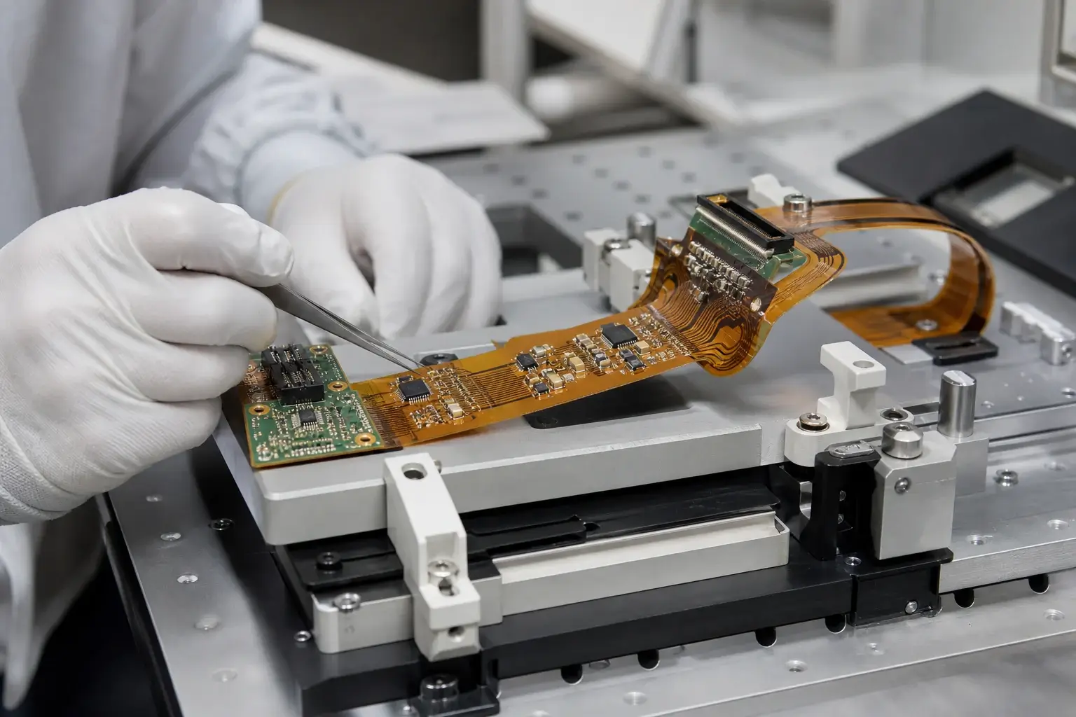
Traceability and Process Control
The traceability chain in flex assembly is a systematic documentation path that begins with the material lot, proceeds through the bare-board lot and assembly lot, and ends with the final assembled product and build revision. Each time a new build is completed, the carrier, stencil, placement, reflow, inspection, and test records document all tool or program IDs and revisions in relation to the actual build revision. When you have a stable production baseline to reference, it is much quicker to diagnose problems in repeat builds by checking the actual materials, tools, and programs to see whether they match the production baseline.
If there is a material substitution, or if you make any changes to geometry, panelization, package, material system, or process parameters during the build process, you must have a documented technical assessment and an updated production baseline.
First-Article and Acceptance Records
First-article records document how each lot or unit ID aligns with the drawing, BOM, build programs, and acceptance class. All deviations must be documented and receive a disposition under the customer acceptance criteria prior to moving forward with the affected build.
Class 2 and Class 3 require that the acceptance standard governing fabrication, assembly, or soldering is properly associated with the records regarding the materials, tools, and processes that support the performance and acceptance of those builds.
Prototype-to-Production Transfer
Prototype settings should move into a controlled production baseline. Preserve these items through the transfer:
- Stackup and material revision
- Panel, carrier, support-insert, and tooling revision
- Stencil revision and solder-paste definition
- Placement program, fiducials, support, and force settings
- Reflow profile record and supported-cooling condition
- SPI/AOI/X-ray inspection program and acceptance revision
- Electrical/FCT fixture and program revision
- First-article record, deviation disposition, and change-control history
The consolidated record connects customer requirements → manufacturing lot → delivery record. Changes to geometry, panelization, package, materials, process parameters, inspection methods, or test programs are assessed, updated, and traceably communicated.
SUGA remains accountable for engineering requirements, stackup and material selection, assembly planning, inspection definition, production records, changes, corrective action, and delivery.
Our PCBA Production Lines
















Flex and Rigid-Flex PCB Assembly FAQs
Flex PCBs can use heavy copper; however, the addition of heavy copper changes the flex construction. The amount of copper affects the thickness of the flex PCB, the neutral-axis position, the minimum bend radius, trace strain, the etching process, coverlay geometry, thermal mass, carrier support, and fatigue performance. You must define copper weight with respect to static or dynamic duty, bend axis, trace direction, layer count, and cycle target. A copper weight of 2 oz does not provide the same bending capability as a thin-copper dynamic flex design.
Yes. Custom flex PCB stackups must clearly indicate the rigid and flex regions, material families, copper type and weight, dielectric and adhesive thicknesses, coverlay, bondply or low-flow prepreg, stiffeners, vias, impedance layers, total thickness, and all revisions. The stackup diagram will be used as the baseline document for fabrication, carrier design, reflow planning, and inspection.
The required annular ring for rigid-flex PCBs can change based on drill diameter versus finished hole, pad size, plating, layer registration, via type, buildup, product class, local density, and fabrication allowance. The value should be established during DFM analysis and confirmed through artwork inspection, dimensional verification, and microsectioning.
Altium or IPC-2581 data may be processed based on whether the project engineering and CAM tools support the actual version and feature set. Fabrication data, BOM, centroid data, drawings, stackup, net information, and revisions must all define the same build.
In some cases. Accessible component, solder-joint, or local pad defects may be repaired only when heat exposure, pad adhesion, cleanliness, flex-zone strain, conductor integrity, and the customer’s acceptance criteria permit it. Creases, edge tears, severe delamination, fractured dynamic-flex conductors, or damage inside a high-strain transition may require replacement. Repaired units should be subjected to documented inspection and electrical or functional verification.
No. Semi-flex is commonly characterized by a controlled, limited-bend region, typically within an FR-4 rigid construction and often achieved by reducing the thickness locally. Conversely, rigid-flex construction consists of true flexible layers, typically polyimide-based, integrated with rigid component regions. FR-4 is not normally used as a continuous-motion flex dielectric. You will choose between semi-flex or rigid-flex based on bending frequency, bend radius, routing method, material thickness, assembly support, and required life validation.