Upload BOM & Gerber
-
Mobile: +86 13312967631
-
Email: sales@sugaintl.com

DFM & DFT Review Services
PCB Design for Manufacturing and Testability
SUGA reviews fabrication limits, assembly access, test-point geometry, fixture clearance, JTAG integrity, and functional-test access as one engineering job.
PCB fabrication, PCBA, fixture, and test resources coordinated through one SUGA engineering team
Physical, logical, programming, and functional access reviewed together
Prioritized findings linked to affected geometry, nets, components, and test methods
What Is a PCB DFM and DFT Review?
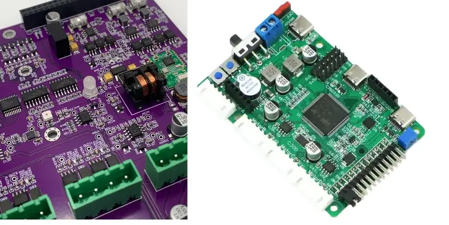
When reviewing PCB DFM, the review determines whether the PCB design can be manufactured consistently. PCB DFT identifies how the PCB can be observed, tested, diagnosed, and programmed. During PCB DFA, the PCB is reviewed to determine whether component placement, soldering, inspection, and repair can occur without interfering with the PCB layout.
SUGA reviews these disciplines together, as a single design decision may affect fabrication, assembly, inspection, and test access. DFMA includes planning for both manufacturing and assembly; however, it cannot replace a full DFT process.
| Design dimension | DFM — Manufacturability | DFT — Testability | DFA — Assemblability |
|---|---|---|---|
| Core objective | Make the PCB manufacturable with stable yield, controlled cost, and repeatable fabrication. | Make the assembled board observable, testable, programmable, and diagnosable. | Make component placement, soldering, inspection, rework, and mechanical integration repeatable. |
| Key inspection items | Trace width/spacing, stackup, via aspect ratio, annular ring, copper balance, panelization, material and finish. | Critical-net access, test-point geometry, fixture clearance, JTAG chain, flying-probe reach, functional-test access. | Component spacing, land patterns, polarity marks, thermal pads, BGA escape, soldering access, inspection visibility. |
| Enabling technologies | Etch compensation, lamination control, drilling, via fill/cap, surface finish, impedance control. | ICT, flying probe, boundary scan/JTAG, programming access, functional test, test fixtures. | SMT, reflow, wave/selective soldering, stencil design, AOI, X-ray, controlled rework. |
| Engineering result | Corrected fabrication data, stackup and material choices, fabrication notes, manufacturable bare-board construction. | Test-access plan, fixture/test method selection, JTAG requirements, coverage gaps with alternate methods. | Assembly-ready land patterns, spacing, orientation, soldering and inspection choices. |
IPC-2221C, IPC-2222B, IPC-6012F, and IPC-7352 are IPC specifications that establish general requirements for PCB design, rigid-board qualification, PCB construction, and land patterns. Likewise, flex and rigid-flex PCBs should be designed in compliance with the applicable IPC flex-board design and qualification specifications. IPC-A-610J and J-STD-001J are specifications for PCB assembly acceptance and soldering processes, while IEEE 1149.1-2013 defines boundary-scan architecture. Ultimately, standards may support PCB DFM and DFT reviews; however, standards are not a substitute for project documentation or the method chosen for PCB manufacture.
PCB Manufacturability Review
PCB DFM transforms the PCB electrical layout into a PCB that can be manufactured consistently through the fabrication process. Just because a PCB layout passes a CAD rule does not mean the PCB has sufficient process margin for etching, lamination, plating, drilling, or solder-mask registration.
PCB Testability Review
A PCB that passes DFM may still be difficult to probe, program, or diagnose. PCB DFT reviews map critical nets and fault classes to the physical locations of pads, exposed vias, component leads, connectors, JTAG connectors, programming interfaces, and functional test access. Board DFT reviews also check the PCB probe travel path, component shadows, PCB clamps, coatings, and enclosure features that have the potential to block planned access points after assembly. Logical access requires a separate review of JTAG, programming, and supported device-level observation paths.
FCT verifies system-level powered behavior that may fall outside the selected structural tests.
Via-in-Pad Process Impact
The escape routes of dense BGA designs demonstrate that DFM, DFT, and DFA cannot be considered independent checklists. The design layout may require the use of via-in-pad or HDI construction to create escape routes. Where solder joints are hidden, X-ray inspection may be necessary to inspect them. JTAG or functional access may also be necessary where probe access is impossible. These choices affect multiple aspects of production.
Potting and conformal coating create a similar interaction. They protect the assembly, but their keep-outs must preserve access to connectors, switches, programming points, and production test points.
PCB DFM Review
All stages of the PCB manufacturing process must be undertaken with consideration of the applicable PCB DFM rules. Minimum trace and spacing rules cover only part of the PCB manufacturing process.
| Design area | Design condition | Failure mechanism | Production consequence | SUGA response |
|---|---|---|---|---|
| Stackup, material, impedance | Dielectric, copper weight, copper profile, layer symmetry or selected material does not match the electrical intent and manufacturing construction. | Lamination movement, copper variation, material substitution or asymmetric construction changes realized geometry. | Impedance drift, warpage, unstable yield or material delay. | Reconcile stackup, material, copper profile, impedance target and manufacturing method before data is finalized. |
| Copper spacing | Copper geometry approaches or exceeds the selected etching window. | Under-etch or over-etch changes conductor width and the remaining isolation between adjacent features. | Shorts, opens, scrap, impedance shift or added processing. | Increase margin or select the manufacturing method matched to the geometry. |
| Pad, component spacing | Land-pattern or component courtyard does not leave stable paste, placement, soldering, inspection and rework space. | Paste interaction, component movement, shadowing or tool obstruction develops during assembly. | Bridging, tombstoning, blocked AOI, manual touch-up or difficult rework. | Adjust land pattern, spacing, orientation, stencil or assembly method. |
| Via-in-pad | A via enters a solderable pad without the required fill, cap and plating construction. | Solder is drawn into the via or the cap/plating interface becomes unstable. | Insufficient solder, voiding, porous joints or reliability loss. | Specify the required filled-and-capped structure and define plating and planarity requirements. |
| Annular ring, drill | Finished hole, drill tolerance and registration leave insufficient copper around the barrel. | The drilled hole removes or weakens the copper connection between pad and barrel. | Intermittent connection, breakout or open circuit. | Adjust pad, finished-hole size, drill tolerance or via construction. |
| Mask, legend, stencil | Mask dam, opening, legend or stencil aperture conflicts with solderable features. | Mask fragments, ink contamination or incorrect paste transfer interferes with solder formation. | Poor wetting, solder bridging, insufficient solder or rework. | Correct mask expansion, legend clearance, stencil aperture and keep-outs. |
| Copper balance, panelization | Copper distribution or panel support creates uneven thermal and mechanical behavior. | Lamination, plating, reflow or handling loads act unevenly across the panel. | Bow, twist, dimensional movement or unstable assembly support. | Balance copper, adjust panel rails, tooling, breakaway method or board support. |
| Assembly access | Tall parts, connectors, dense placement or enclosure features block placement, inspection, soldering or repair. | Equipment, camera, nozzle, soldering tool or rework tool cannot reach the target feature. | Slower production, hidden defects, manual intervention or limited repairability. | Adjust orientation, spacing, assembly sequence or process selection. |
| Assembly material readiness | Specified part, package, or alternate is unavailable or mismatched to the land pattern or assembly process. | A substitution changes pad fit, polarity, thermal behavior, inspection access, or process settings. | Assembly interruption, redesign, or uncontrolled sourcing change. | Confirm part numbers, package compatibility, and approved alternate criteria before release. |
| Special processes | Non-standard via, finish, coating, potting, material or panel requirement is not identified early. | The required capability is discovered after files and materials are committed. | Added process steps, material changes, delay or redesign. | Define the manufacturing method and documentation. |
| Test interaction | Manufacturing geometry blocks critical-net probing or adds stubs to sensitive channels. | The DFM solution creates a new DFT or signal-integrity conflict. | Limited coverage, false failures or channel degradation. | Coordinate fabrication geometry with the selected probing strategy and electrical requirement. |
PCB Stackup Review
A design tool’s nominal stackup is only a starting point. Even when every layer matches the drawing, variations in resin lots, press-cycle conditions, or copper-foil profiles can shift the final dielectric and impedance characteristics of a PCB and its final performance. For high-speed channels, loss tangent, conductor roughness, glass type, connector transitions, and the selected test structures can shift the actual performance of the PCB away from its nominal performance.
The selected manufacturing method must not only ensure that the PCB meets its electrical requirements but also allow adequate access for validating results without introducing additional stubs.
PCB Spacing Control
At the initial layout stage, spacing ranges such as copper spacing, pad spacing, and component spacing are often established as a single “clearance” dimension, although they affect different manufacturing steps independently. For instance, an etch-safe copper gap does not indicate whether the paste stencil has sufficient room to print cleanly, nor does a stencil-safe pad pitch indicate whether a rework tool has room to reach the joint after the component has been soldered.
It is possible for a design to meet the electrical clearance criteria but still have insufficient manufacturing margin. SUGA separates electrical clearances from manufacturing margins so corrections can be directed to the actual issue, whether that requires an increase in geometry margin or a manufacturing process matched to the feature density.

PCB Via Design
A via-in-pad structure has four disciplines governing it: drilling establishes the barrel, plating creates the cap, soldering determines whether solder wicks into the barrel instead of forming the joint, and testing determines whether a test probe can still contact the remaining pad area. Treating only one of the four disciplines in isolation may produce a via that passes fabrication drawings but ultimately fails during assembly or testing.
In addition, high-speed vias require decisions regarding stubs and backdrilling. Backdrilling is used only when the channel and construction require it; it is not an automatic choice for every fast signal. When a via cannot provide stable probe access, the test point shifts to a dedicated pad, connector, JTAG path, or another controlled access method.

Solder Mask and Stencil Review
Before assembly, the mask and stencil information is considered complete, and mismatches rarely appear as rule exceptions until paste is on the pad and a defect is discovered. For example, a stencil aperture that is undersized for a thermal pad will decrease the amount of solder available at the joint, and the issue may go unnoticed until voiding is detected in the joint. Similarly, legend ink that spreads onto a solderable pad will decrease the likelihood of correct solder wetting. The only way to catch both cases correctly is to review the stencil and legend data against the physical land pattern, not just the nominal aperture ratio.
During this review, component polarity and designator visibility are preserved, while coating, potting, and adhesive are kept away from connectors, switches, test points, and repair locations.
Assembly Access
Assembly access must follow the established assembly sequence. An item that is accessible at the beginning of assembly may become inaccessible after a taller item or connector is assembled next to it.
The assembly access review must consider proper clearance for the planned assembly and rework sequence, not just the static footprint. Access for both AOI and X-ray inspections is also based on the package type placed on the board and the visibility of its solder joints. There is no single inspection rule for every component on the board.
PCB DFT Review
PCB Test Point Geometry
The geometries assigned to PCB test-point access should be based on the required nets and fault classes rather than raw test-point counts. The access plan establishes a consistent primary probe side; access from both sides is added only when component placement or the required coverage makes it necessary.
The dimensions for test pads are intended to provide preliminary design targets. The final geometry will be determined based on the test type, probe and receptacle family, tip style, spring force required to maintain contact, surface finish, clearance, and support under the assembled board. Test points must remain clear of clamps, tooling holes, panel rails, and handling zones so that PCB support and probing do not compete for the same space.
| Geometry field | Access configuration | Preliminary design target | Preferred target | Design constraint |
|---|---|---|---|---|
| Pad diameter | Bed-of-nails ICT | 0.8 mm (32 mil) | 1.0 mm (40 mil) | Stable board support and sufficient component clearance. |
| Pad diameter | Flying probe | 0.5 mm (20 mil) | 0.75 mm (30 mil) | The target pad, surface finish, and assembled-board clearance support repeatable contact. |
| Pad diameter | Manual probing | 1.0 mm (40 mil) | 1.5 mm (60 mil) | Debug or controlled manual measurement with operator/tool access. |
| Center spacing | Bed-of-nails, standard probes | 2.5 mm (≈98 mil) | 2.54 mm (100 mil) grid | Standard grid with sufficient board support and component clearance. |
| Center spacing | Bed-of-nails, fine probes | 1.8 mm (≈71 mil) | 2.0 mm (≈79 mil) | Fine-pitch access with defined mechanical support. |
| Center spacing | Flying probe | 1.5 mm (≈59 mil) | 2.0 mm (≈79 mil) | Adjacent-component and height clearance remain available. |
| Center spacing | High-density special probes | 1.27 mm (50 mil) | 1.5 mm (≈59 mil) | Specialized access is selected for the board. |
For repeated fixture points, a consistent base grid improves probe layout, probe replacement, and fixture maintenance.
The fixture design should account for both board deflection and support-pin placement to ensure that access to dense areas does not interfere with stable contact.
Critical-Net Access
Coverage for critical nets includes identifying the nets and fault classes that are meaningful to the design. These include power rails, ground references, clocks, resets, programming lines, communication buses, control signals, and failure-sensitive analog nets; each must have a physical or logical observation method. A net can only be unavailable for physical access if another named access method covers the required fault or function.
Physical and Logical Access
Access methods include both physical and logical access, with physical access provided through dedicated test pads, untented vias, through-hole leads, and controlled SMD pad extensions. Dedicated pads provide a reliable physical connection for production testing. Vias and pad extensions take up less board area than dedicated pads, but they must maintain solderability, impedance, surface finish, and probe clearance.
Connectors and headers provide access for programming, debugging, or functional testing, whereas JTAG provides logical access through compatible devices. Every physical access point should remain accessible following assembly, coating, board support, and enclosure integration.
Test Coverage
Test coverage separates three elements: physical access to the nets, structural fault coverage, and functional verification. The number of test points does not guarantee access to the appropriate nets or product behaviors. Accessible opens and shorts can use Flying Probe or ICT; supported dense interconnects can use boundary scan; and powered analog, communication, or load behavior requires functional verification.
Test Method by Production Volume
Fixtureless probing supports prototypes and designs with frequent revisions without requiring dedicated fixtures. ICT becomes practical when the design, access geometry, and production volume justify fixture engineering, maintenance, and faster repeated cycles. When the chain remains stable, boundary scan supports compatible interconnects and programming.
The length of time required for functional testing is determined by the interface, load, and stabilization sequence.
Complex assemblies combine different methods by fault category when one method cannot provide all the coverage required for the entire assembly.
JTAG Test Access
To use a JTAG chain effectively, the devices in the chain must be compatible, the correct BSDL files and device order must be defined, TDI/TDO connections must be continuous, TCK and TMS signals must be stable, reference voltage and ground must match, reset and bypass handling must be defined, and connector mapping must be accessible. Devices with AC-coupled or differential interconnects may require IEEE 1149.6 or another suitable test-access method.
Boundary scan can be used to test supported BGA and interconnect faults or perform programming functions. However, boundary scan cannot verify analog performance or provide a complete view of overall product behavior. Programming and debug interfaces can only be shared if their operating voltage, security, and production-control requirements are compatible.
DFM and DFT Review Process
The review process begins while the stackup, placement, and test access are still adjustable. It then aligns the manufacturing data set, qualifies automated findings, assigns severity levels, and resolves the resulting production and test requirements through corrective actions.
When Should a PCB DFM Review Start?
The first review should commence while the schematic intent, preliminary stackup, critical part placement, placement restrictions, key interfaces, and anticipated test method are still adjustable. After detailed placement and routing checks, a final review of the fabrication, assembly, and test information is completed to ensure consistency before manufacturing or fixture programming begins.
Corrections made at the beginning of a project remain within the design data. Once issues arise during quotation, fabrication, assembly, or testing, changes may affect routing, construction materials, fixtures, completed hardware, electrical performance, and the delivery schedule. Consequently, logical and physical test access must be specified together with component placement and routing.
PCB Design Files
PCB design files include the files that define the construction of the PCB. Gerber RS-274X, ODB++/IPC-2581 data, NC drill data, and the drill map establish the PCB fabrication geometry. The stackup, construction materials, copper profile and weight, and impedance requirements form the basis for the intended PCB construction.
In addition, the PCB schematic identifies critical nets and connections that cannot be determined from the manufacturing data alone. All files listed here should be compiled into one review data set with aligned revisions and defined manufacturing and testing methods.
Assembly Test Data
The assembly test data accompanying the BOM also identifies the designated manufacturer part numbers. This information confirms component identity, land-pattern compatibility, orientation or polarity, and package assembly requirements. Centroid data, the assembly drawing, and special process notes also support soldering and placement checks.
ICT, flying probe, JTAG, programming, FCT, connector, load, coating, potting, enclosure, keep-out, and fixture requirements define the applicable mechanical and test constraints.

PCB Production Blockers
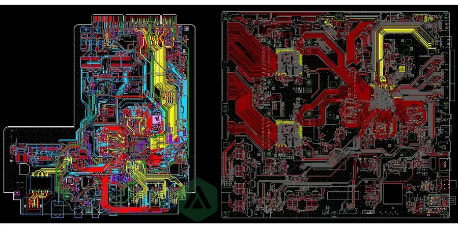
The first step in identifying production blockers is automated rule-based detection of geometry, nets, drills, masks, component clearance, panel usage, and other obvious conflicts. After automated detection, engineering analysis qualifies the findings against the original electrical intent of the PCB design, stackup, copper balance, via construction, construction materials, SI/PI interaction, assembly access, probe access, and test-method coverage.
After the findings are qualified, they are sorted into production blockers, reliability risks, and optimization items. A prioritized list of corrections is then generated.
Each identified finding documents the affected layer, net, component, or process; the severity rating of the issue; and the recommended design correction, supported manufacturing method, or alternative assembly or test strategy.
Production Data Alignment
The review of the PCB design files produces updated design files for PCB manufacturing, as well as updated test requirements. SUGA aligns critical geometry and stackup changes, via and mask requirements, stencil and assembly access, test-point geometry, JTAG access, data-set consistency, manufacturing feasibility, and alternative coverage for areas where direct probes are not accessible.
Review Deliverables
The review package separates production blockers, reliability risks, and optimization items and identifies the affected geometry, net, component, or process. It also provides the recommended correction or supported method for resolving each finding, as well as alternative coverage where direct probe access is unavailable. Revised fabrication notes, assembly constraints, and test requirements remain connected to the same revision of the production files.
DFM Software vs. Engineering Judgment
While many PCB DFM software products perform well at repeatable checks against geometry, drill, mask, net, and component-clearance rules, they do not determine whether identified features maintain the original electrical intent, comply with the selected manufacturing method, or require an alternative assembly or test strategy. SUGA combines automated analysis with engineering judgment for this reason.
| Analysis area | Automated finding | Engineering interpretation required |
|---|---|---|
| File recognition | Layer, drill, net, mask and outline identification | Establish intended layer function, revision consistency and missing design information. |
| Geometry rules | Trace/space, annular ring, drill, mask and edge-clearance flags | Match rules to the selected manufacturing method, material, copper weight and reliability requirement. |
| Net comparison | Opens, shorts and connectivity mismatches between data sets | Resolve intentional net ties, component behavior and schematic/manufacturing-data conflicts. |
| Drill/via analysis | Via type, drill size, aspect, annular-ring and via-in-pad flags | Select via construction, fill/cap, plating, backdrill and test-access treatment. |
| Component clearance | Courtyard, body, height and orientation conflicts | Account for placement equipment, AOI, X-ray, soldering, enclosure, fixture and rework access. |
| 3D preview | Mechanical and placement visualization | Match component models, connector mating, enclosure and process-tool access. |
| Panelization | Board count, rails, tooling and material utilization | Balance material use with support, depanelization, fiducials, test access and assembly stability. |
| Testability rules | Missing or inaccessible points, spacing and component obstruction | Map physical access to fault categories, JTAG, programming and FCT. |
| Cost/process flags | Non-standard geometry or process indicators | Decide whether to modify the design or use a manufacturing method that supports the requirement. |
Applications
In high-speed channels, the probe structure is typically restricted; coatings conceal access; and isolation creates separate reference domains. Dense layouts often limit the overall coverage to connectors, boundary scan, or functional fixtures. The review process must preserve all of the dominant electrical, mechanical, and environmental requirements while maintaining the ability to diagnose production defects.
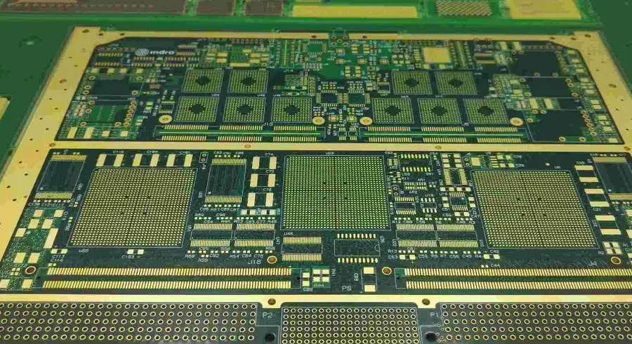
High-Speed Data Center PCB
Across 28, 56, 112, and emerging 224 Gb/s-per-lane classes, a via stub that was harmless at 56 Gb/s can become a return-loss failure if the same layout is reused at 112 Gb/s or 224 Gb/s without revalidating the backdrill depth and reference continuity from the PCBA to the test connector. Using the SUGA process, the dielectric thickness, low-loss material, and connector breakout are matched to the actual lane rate rather than the rate used for the original stackup. Validation at the connector is necessary when the probe branch will affect channel margin. DFT allows continued access to clock, power, and programming without introducing discontinuities.
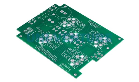
Automotive Control PCB
The layout of an automotive control PCB is heavily influenced by connector loads, power distribution, thermal cycling, vibration, coatings, and long service life. A common failure mode is a BGA or connector joint that is functional during initial testing but fails after several cycles of thermal expansion and contraction. The SUGA process evaluates the robustness of vias and solder joints against the duty cycle rather than simply following placement rules. Once the coverage requirements for the power rails and critical I/O have been identified, functional coverage can be determined before applying coating, allowing continued diagnosis of load-transient, interconnect, and connector faults after assembly.
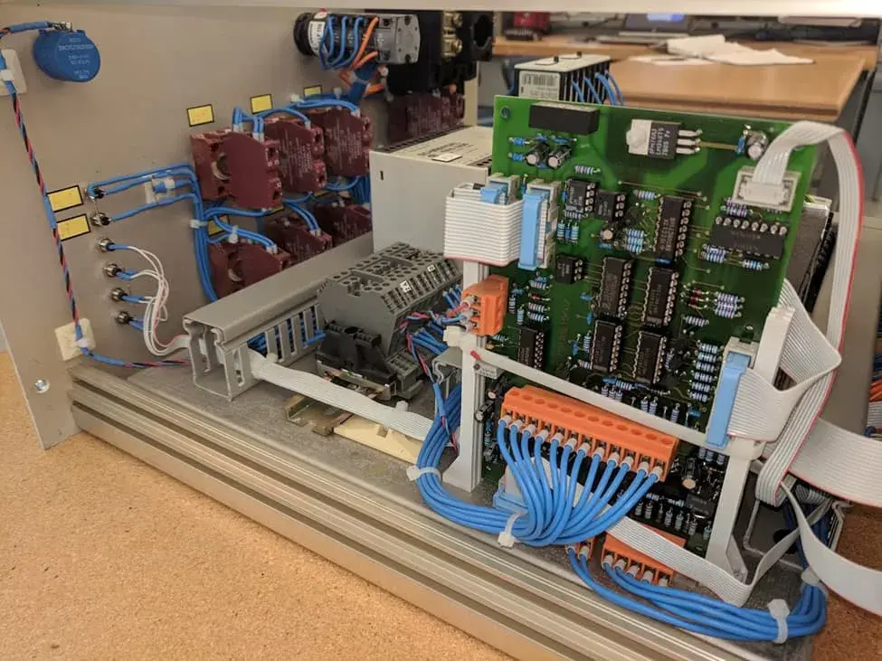
Industrial Automation PCB
Field wiring, isolation, continuous operation, electrical noise, coatings, and service diagnostics are all factors affecting the review of an industrial automation PCB. The recurring risk remains the same: two isolation domains may share a common reference through the fixture itself. A probe or ground clip on one isolation domain may silently create a short circuit to another isolation domain. Therefore, DFM and DFT address the risk differently: DFM verifies creepage for each domain, whereas DFT assigns the correct ground and load conditions domain by domain rather than through one fixture-wide reference. Analog and digital I/O remain visible after assembly without a shared-reference risk.
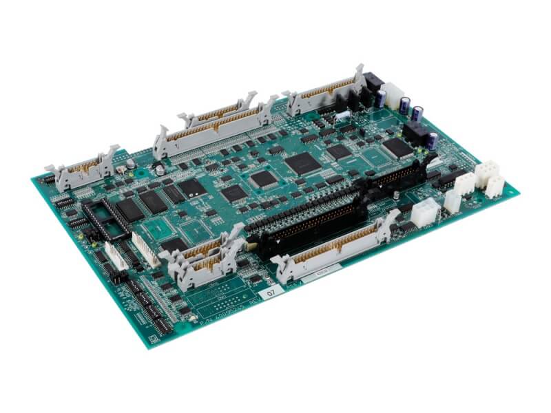
Energy and Power Electronics PCB
High current, high voltage, switching edges, magnetic components, thermal concentration, and isolation barriers make test access a safety and layout decision: a fixed probe location adjacent to a switching node can itself become a clearance violation. DFM examines the copper cross-section where the probe would touch. DFT establishes separate measurement protocols for low-voltage control tests and energized measurements. Whenever a fixed probe location reduces clearance or exposes personnel to stored energy, DFT directs the use of connectors instead.
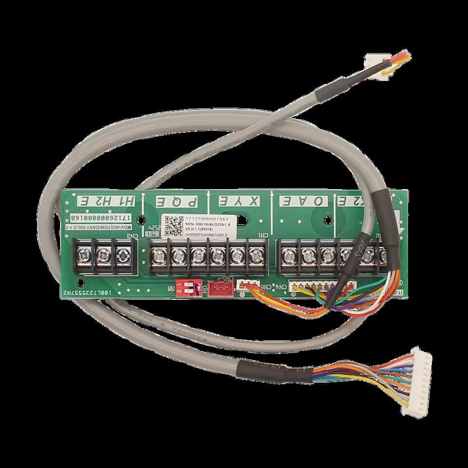
Outdoor Communication PCB
Moisture protection using coatings, seals, potting, and combined high-speed and power interfaces may conceal test access before final assembly is completed. SUGA times the test plan to account for those conditions: pre-coating access covers structural faults, while temporary masking or sealed connectors are used after coating to verify points where permanent pads have been sealed over. High-speed interfaces are kept free from probe branches created by rushed pre-coating testing.
Consumer Electronics PCB
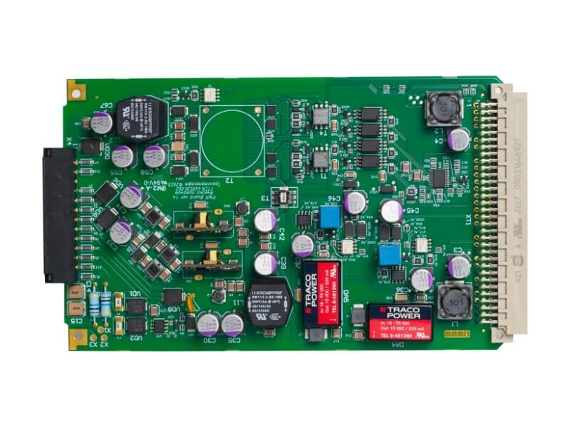
Tight design geometries, fine-pitch components, small connectors, antennas, batteries, and frequent design changes reduce the allowable manufacturing margin for nearly all types of consumer electronics. The most extreme case occurs with batteries and radios: the enclosure and antenna keep-outs may be finalized late, leaving no space to install permanent pads on the RF board. This forces calibration and RF testing to occur through connectors that were defined before production. DFM reviews land patterns and rework access. DFT provides access to power, charging, display, and wireless signals through probes, connectors, or JTAG interfaces sized to the reduced footprint of these products.

Medical Device PCB
Risk-based verification and traceable production information shape the review more than raw defect rate. Medical device PCBs need to provide a test interface for verifying calibration and alarm-path behavior without compromising device cleanliness or enclosure integrity; therefore, common access-point locations may be ruled out. SUGA examines material stability and traceable production information. DFT defines an appropriate alternative access or verification method for power, sensors, and alarms when direct probing is not appropriate.
Aerospace/Defense PCB
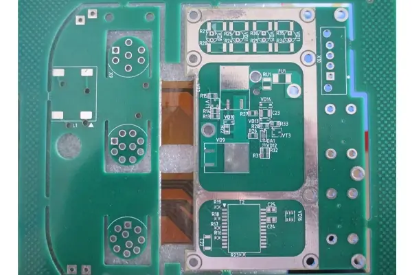
Vibration, thermal cycling, controlled configuration, non-visible joints, coating, and limited field access cause the greatest expense when a fault occurs later in the cycle. Staking or coating can seal previously used access points before anyone knows that they were the only routes to a critical net. This means that structural testing is assigned before staking or coating, or moved to retained connectors. DFM reviews stackup stability and barrel robustness; DFT defines alternate connections for critical nets, JTAG devices, and final functional verification.
DFM and DFT Review Cost and Production Impact
Design-stage findings impact CAD data, stackup configuration, material selection, spacing requirements, via locations, masking processes, assembly choices, and test-access design. After board assembly, the same design corrections can impact fabricated boards, components, solder joints, process instructions, fixture requirements, rework labor, and material containment.
System integration includes fault isolation involving firmware, cables, enclosures, multiple boards, and system interfaces. Discoveries made in the field can include installed products, service labor, downtime, returns, and issues that could lead to long-term reliability exposure.
Having planned test access on a board will assist in identifying faults on the board and isolating them from interactions with other components or subsystems. The corrective action associated with the diagnosed fault must address the root cause of the defect at the design, fabrication, assembly, or testing level. If test access is not available on a board, the associated debug costs will increase because it will be more difficult to isolate component, solder-joint, interconnect, firmware, and system faults.
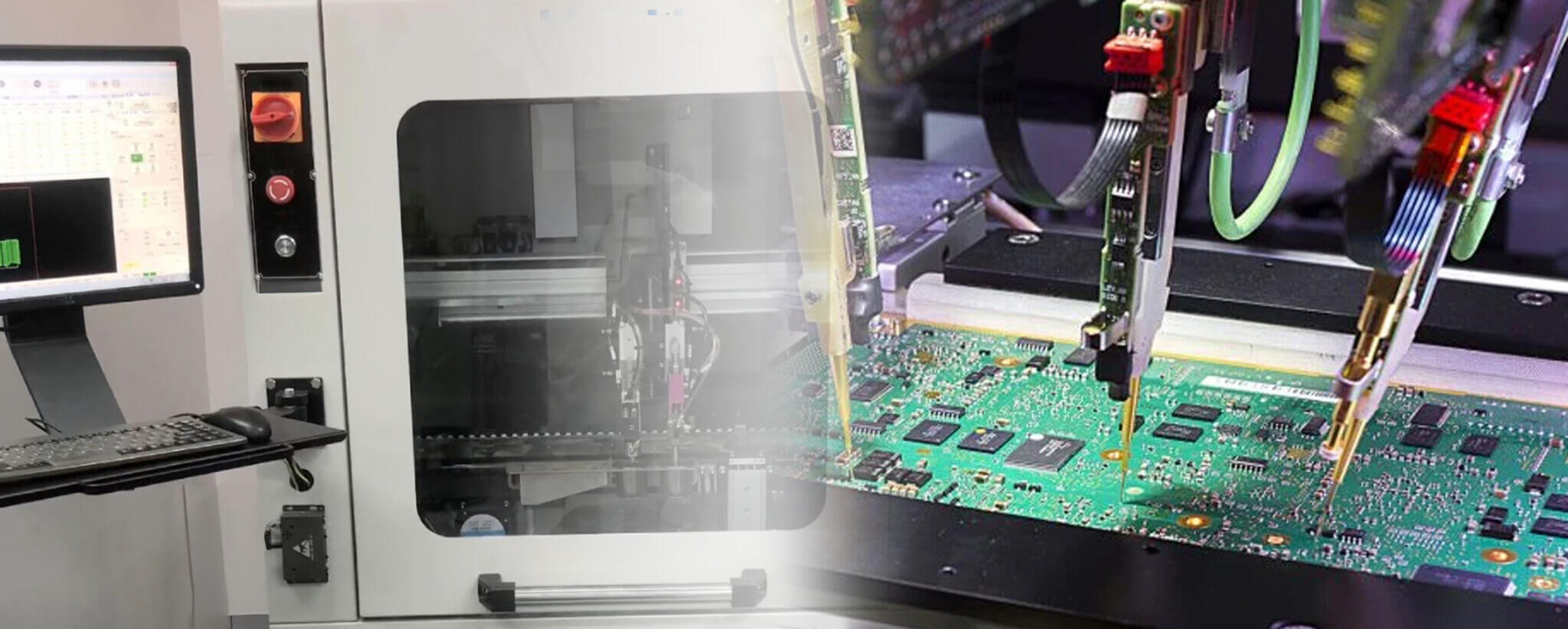
Our PCBA Production Lines
















DFM and DFT Review FAQ
During a review, the reviewer will typically use Gerber RS-274X or ODB++/IPC-2581 data, NC drill files, stackup configuration, the schematic, BOM, centroid data, the assembly drawing, and test requirements. The specific set of files used to conduct the review will be determined based on the particular construction of the board and the level of test coverage required.
A fabrication-only review will be completed more quickly than a combined DFM, DFA, and DFT review. Timing will increase when the data set includes unresolved revisions, HDI or rigid-flex construction, high-density double-sided assembly, controlled impedance, JTAG, fixtures, or functional-test requirements. SUGA will confirm the DFM review schedule once file completeness and review depth have been verified and will also separate the time for the first findings cycle from the customer’s correction time and resubmission time for review.
For prototypes and frequently revised boards, Flying Probe is usually a good option because it does not require a dedicated fixture. Stable production may justify the use of ICT when test-point access density, test volume, per-board cycle time, fixture engineering, and maintenance support the costs associated with ICT. JTAG or functional testing may also be used for supported hidden interconnects, firmware programming, and powered behavior that structural probing cannot cover.
PCB test coverage generally defines the required fault classes and functions in the test-coverage map and matches them to physical access, logical access, programming, or functional verification. The test-coverage map will include alternative methods where direct probing is not possible rather than simply calculating a raw test-point percentage.
The PCB DFM and DFT review cost is based on board-construction complexity, layer count, material and stackup maturity, the level of HDI or rigid-flex construction, assembly density, required test methods, fixture and programming requirements, file consistency, and corrective-engineering depth. The cost of the engineering review is separate from the cost of fabrication, fixture construction, and production testing.