Upload BOM & Gerber
-
Mobile: +86 13312967631
-
Email: sales@sugaintl.com

Lead-Free PCB Assembly Services
Lead-Free PCBA Manufacturing in China for RoHS-Compliant Electronics
Lead-free PCB assembly covers every step from solder-alloy selection to final PCBA inspection under RoHS and REACH. SUGA runs lead-free SMT, PTH, wave, reflow, selective, and manual soldering, with compliance records, thermal-process control, and solder-joint reliability checks built into each build.
6 Assembly Processes
SMT · PTH · Manual · Reflow · Wave · Selective
5 Inspection Methods
Electrical Test · AOI · X-Ray · ICT · FCT
10 Restricted Substances
RoHS 3 Compliance Scope
240–260°C Reflow Window
Lead-Free SAC Process Control
What Is Lead-Free PCB Assembly?
Lead-free PCB assembly is a type of PCB assembly built using lead-free solder materials, soldering processes that have been controlled in a compliant manner, and an inspection process to ensure the final PCB assembly itself meets the requirements set forth by RoHS/REACH-bound electronics. "Lead-free" refers to compliance with RoHS requirements, not a clean or pure lead-free product. RoHS establishes a maximum lead concentration limit of 1000 ppm (<0.1% by weight in homogeneous material). Therefore, even though a finished PCB assembly may contain trace lead from the plating process, components, or alloy impurities, it is not disqualified from being compliant under RoHS.
What Controls The Finished Assembly?
Control of the finished assembly for a lead-free PCB assembly project is achieved by the assembled PCB itself; however, it is not limited to the assembled PCB, as it includes the solder material used, the PCB finish, the components used, the BOM, the MBR for the assembled PCB, and the inspection/verification record for the finished PCB assembly. Each of these items for the finished PCBA must link back to the same job and lot number.
The finished assembly will be considered compliant to RoHS and REACH based on the soldering process and the components used, not necessarily the bare PCB. Therefore, the assembly decision should take into account the compliance status and how the solder joints will perform on the delivered PCB assembly.
Where Lead-Free Compliance Gets Triggered
There are three main factors that can trigger compliance with lead-free PCBA: regulatory compliance (the product entering a market subject to RoHS/REACH regulations), contractual compliance (a customer's specification on restricted substances), and policy compliance (a brand's requirement for environmental compliance before shipping).
Electronics used in automotive, medical, industrial, IoT, and lighting applications usually experience multiple triggers simultaneously, and these combinations affect the acceptance criteria in each application sector.
What Counts As RoHS-Compliant PCBA
PCBAs that are RoHS-compliant are assessed based on their compliance with the limits on restricted substances, material declarations, solder-selection specifications, assembly-process history, and final assembly documentation. The same lead limit defined above establishes the baseline for each build. However, the lead limit is recorded within the job record linked to a specific production lot, solder alloy, and BOM revision; it should not exist as a separate item in the environmental claim.
How Compliance Evidence Follows The Assembly
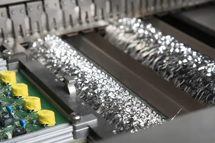
The compliance records for RoHS-compliant PCBA are maintained for the entire PCBA manufacturing process. PCBAs must have their restricted-substance compliance established before selecting the solder type and preparing their BOM. PCBAs have their compliance established through records of restricted-substance usage, solder type used, BOM status at first assembly, PCB finish type, production process notes, and associated shipping documents. PCBAs are subject to restrictions from RoHS on the substances allowed in the electronic product and its production materials; REACH specifies the duties and responsibilities for chemical substances regarding safety and safe use.
Restricted Substances
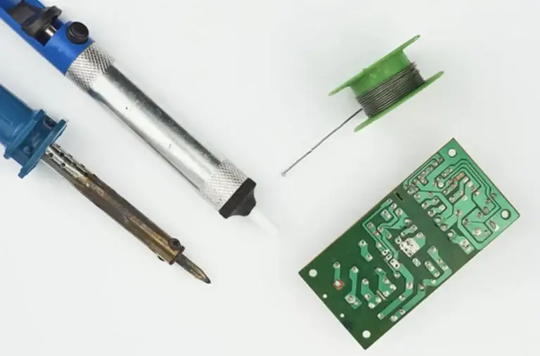
RoHS prescribes a limit on each of the 10 substances it restricts: lead (Pb), cadmium (Cd), mercury (Hg), hexavalent chromium (Cr6+), PBB, PBDE, and the four phthalates: DEHP, BBP, DBP, and DIBP (Directive 2015/863, RoHS 3). The lead and cadmium limits are the common checks at the PCB assembly level for the process and sourcing groups, and, as noted, they apply to entirely different material areas; lead applies to the soldering process, whereas cadmium is typically found in plating, pigments, and finish coatings rather than in the solder joint itself.
This difference in compliance risk will determine where the issue actually lies: for instance, switching to SAC305 for the solder alloy will meet the lead limit; however, using an older style of connector plating or a low-cost pigment may inadvertently lead to a failure to meet the tighter cadmium limit even after the solder meets compliance. Because of this, plating and pigment sourcing must also be documented separately from the initial approval of the solder alloy. The table below shows the specific limits for each of the prohibited substances as well as where each is found on the finished assembly.
| Control item | Engineering check | Record | Manufacturing note |
|---|---|---|---|
| Lead limit | Verify the PCBA against the RoHS lead limit | Lead content below 1000 ppm (<0.1%); 0.1% by weight in homogeneous material | Applies to solder alloy, termination finish, and any leaded legacy components sharing the line. |
| Cadmium limit | Verify plating, pigments, and contact finishes against the stricter cadmium limit | Cadmium content below 100 ppm (0.01% by weight) | Most often surfaces in connector plating and colorants, not in the solder joint itself. |
| RoHS substance scope | Check solder, PCB finish, components, and assembly materials | RoHS compliant PCB assembly | Lead and cadmium drive the soldering discussion; Hg, Cr6+, PBB/PBDE and four phthalates fall under the same directive at 1000 ppm each. |
| REACH declaration | Confirm chemical-substance responsibility where required | RoHS and REACH compliant | Runs alongside RoHS and covers SVHC substances not enumerated on the RoHS restricted list. |
| WEEE context | Identify waste-electronics market context where relevant | WEEE context | Treat as market context, not soldering evidence. |
| CoC / material declaration | Tie compliance documents to BOM and material status | CoC and compliance evidence | Match the record to BOM, solder alloy, PCB finish, and assembly lot. |
| Labeling / trace mark | Keep lead-free assemblies identifiable where required | Required labeling for lead-free PCB assemblies | Marking can sit on the board, package, traveler, or shipment document. |
| Quality record | Support recognized quality and workmanship standards | ISO9001:2015 Certified; UL Listed | ISO9001:2015 governs the QMS; IPC-A-610J / J-STD-001J (when specified) governs workmanship acceptance — cite both, not just one. |
Lot-Level Compliance Records
For procurement and quality teams, the compliance record for lead-free PCBA follows the delivered lot, including the solder alloy, PCB finish, and components, and is associated with one lot number as opposed to being distributed as a standard set of documentation.
Export Market Access
RoHS-compliant PCBA supports components entering markets in which restricted-substance controls, material-source evidence, labeling, and other environmental policies will affect the selection of suppliers. Most commonly, EU market access is the motivation for using RoHS-compliant PCBA. For projects in the United States, most often the customer specifications, state restricted-substance regulations, or corporate policies regarding the environment are the drivers of using RoHS-compliant PCBA rather than a federal requirement for RoHS compliance.
Lead-Free Solder Materials and Process Controls
When using lead-free solder, a reliable solder joint can be made when the selection of solder alloy, SAC or SnCu, paste-handling procedures, flux system, PCB finish, and thermal processing are controlled as a single build condition. Lead-free PCBA typically uses either SAC or SnCu solder alloys, and which is the correct alloy depends on the soldering type, such as SMT paste, wave, selective, or manual, the tolerance of the components, the thermal mass of the PCB, and the finish used.
| Process item | Engineering value | Use point | Control impact |
|---|---|---|---|
| RoHS lead limit | Lead content below 1000 ppm (<0.1%) | Compliance anchor before solder selection | Material choice must support the defined RoHS threshold. |
| SAC305 alloy | Tin: 96.5%, Silver: 3%, Copper: 0.5%; eutectic melting point ~217–220°C | Lead-free alloy for SMT reflow | Affects melting range, wetting, reflow setup, and cost. |
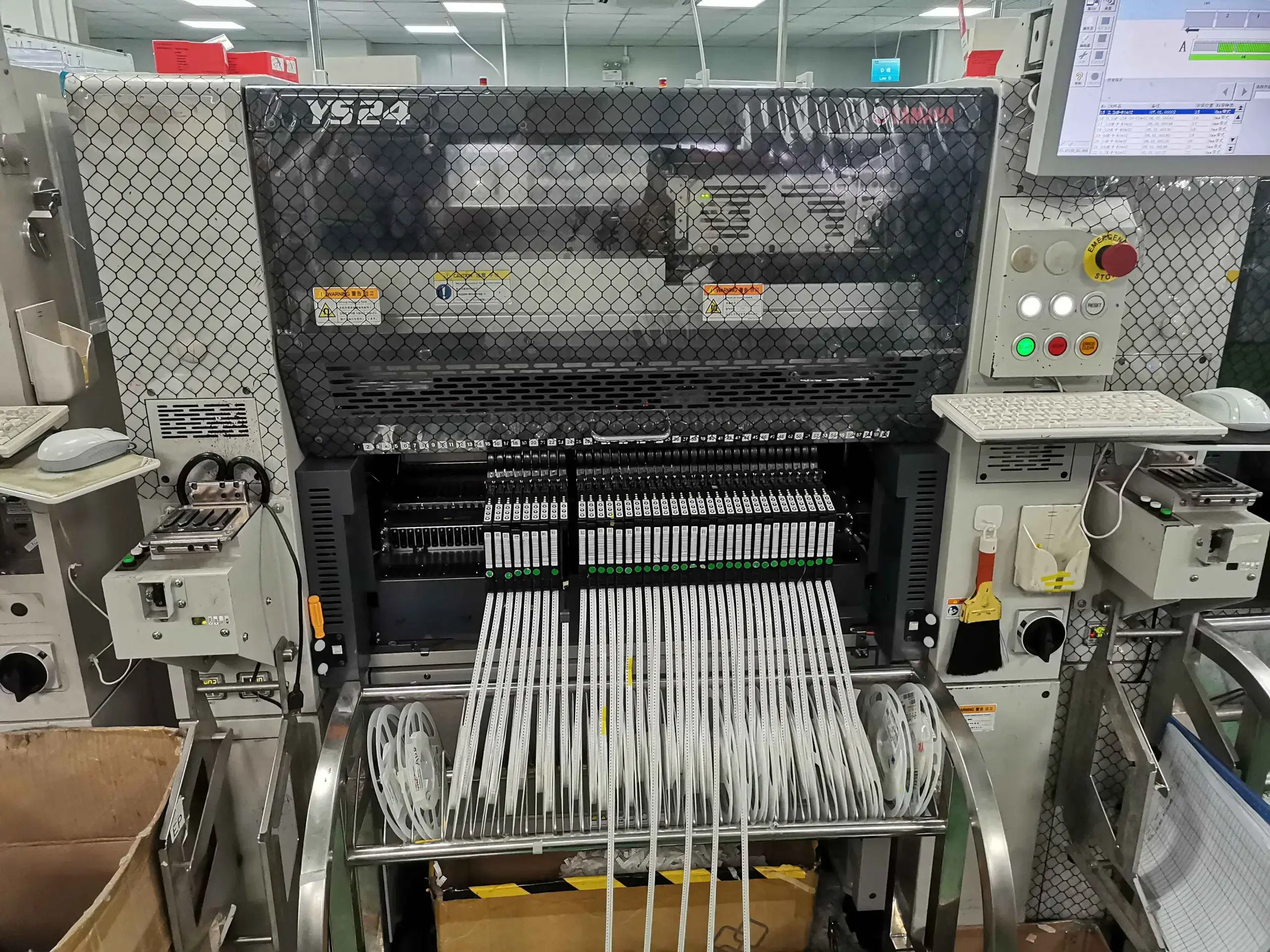
| SMT solder paste | 95.5 Sn/4.0 Ag/0.5 Cu or 96.5 Sn/3.5 Ag | SMT printing and reflow | Match paste to stencil, flux system, placement, and profile. |
| Wave solder bar | 99.3 Sn/0.7 Cu | PTH and wave soldering | Requires a process window separate from SMT paste. |
| Soldering wire | 99.3 Sn/0.7 Cu | Manual soldering and rework | Keep touch-up material compatible with the lead-free build. |
| Solder paste handling | 2–8°C storage / 22–28°C use | Storage, thawing, and use control | Controls print stability, tack life, solderability, and defect risk. |
| Flux / residue control | Flux must match paste, cleaning, and ionic cleanliness needs | Flux and residue decision | Impacts wetting, residue, corrosion risk, and cleaning method. |
| Wave / selective solder pot temperature | 250–280°C, measured at the pot — a separate reference point from reflow peak | Wave and selective soldering pot temperature | Check pot temperature against pad thermal mass and dwell time. |
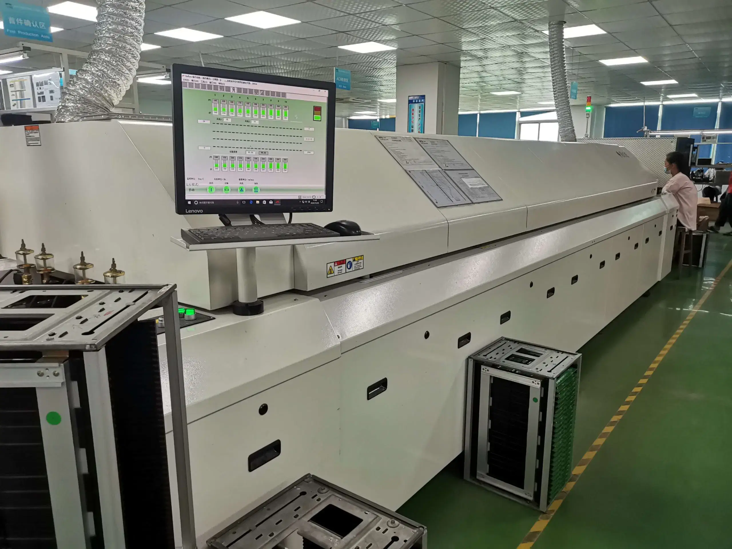
| Reflow condition example | 150–180°C preheat / 240–260°C peak / 30–90 seconds | Reflow window for SAC alloys | Tune by board design, component mix, MSL status, paste, and package limits. |
| Lead-free HASL | Lead-free HASL finish | HASL finish option | Check flatness, thermal exposure, storage, and package pitch. |
| OSP finish handling | OSP vacuum packed / quick assembly / no bake before assembly | OSP storage and assembly timing | Controls oxidation risk, bake decision, and assembly timing. |
| ENIG / other finishes | ENIG supports solderability and flatness when specified | Finish option for fine-pitch or storage needs | Select by pitch, shelf life, cost, solderability, and inspection need. |
Lead-Free Solder Alloys
SAC305 (Sn96.5/Ag3.0/Cu0.5) is SUGA's standard lead-free solder for SMT reflow processes, while SnCu alloy (generally Sn99.3/Cu0.7) matches wave soldering and solder wire applications. These alloys define wetting characteristics, thermal properties, and compatibility for touch-up soldering operations; therefore, SUGA utilizes the preferred soldering method in combination with the corresponding solder alloy for each soldering step, i.e., SAC alloy paste for reflow, SnCu solder bar for wave soldering, and SnCu solder wire for touch-up soldering. This avoids forcing one alloy designation across the entire PCB.
How Paste Handling Affects Soldering
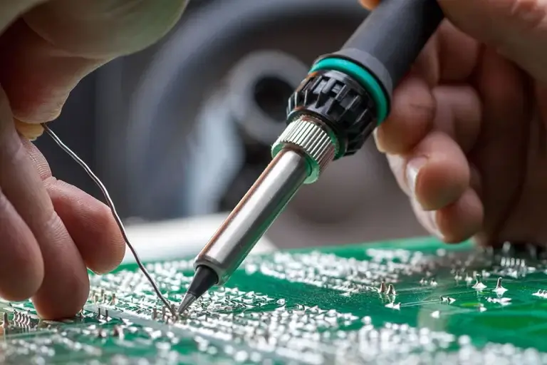
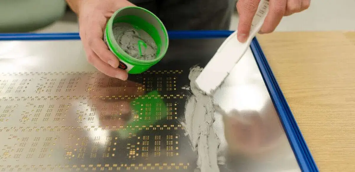
Before being processed through a reflow oven, solder paste is delicate and can be adversely affected by rapid temperature increases, excessive exposure time, or printing outside the accepted stencil print window. If any of these occur, the result can be inadequate solder, solder bridging, or poor wetting; thaw time, acceptable print times, stencil print window, and stencil print placement must all fall within the usable paste window. Only storing at the appropriate solder paste temperature does not guarantee that an acceptable joint can be formed to meet requirements.
Flux handling requires similar diligence; the flux used must be matched to the solder paste system, the cleaning process, and the ionic cleanliness target for the assembly. It is easy to use no-clean flux; however, excess flux residue must also be suitable for the operating environment of the product.
Surface Finish Choices
Surface finish can affect solderability, storage ability, and thermal properties of the printed circuit assembly. Lead-free HASL is a suitable surface finish option for assemblies with a component pitch and thermal exposure that permit hot-air leveling; OSP can also be considered an assembly timing option, because it protects the exposed copper pads until the assembly has been completed.
When considering fine-pitch or storage-sensitive assemblies, ENIG should be the preferred surface finish option. For these products, flatness, shelf life, and solderability are paramount to the assembly process.
Which Temperature Window Fits The Board?
The lead-free soldering process has a higher thermal window than that used during lead-based solder processing. The two most popular lead-free soldering methods are wave soldering and selective soldering, and both have different temperature reference points. Wave and selective soldering generally use a solder pot temperature of 250–280 degrees Celsius, whereas the peak temperature for SAC alloy during reflow is usually between 240–260 degrees Celsius for a period of 30–90 seconds. The process temperature table provides a guideline for these two groups of data. Regardless of which method is used, the final reflow profile still depends on several factors, including PCB mass, component mix, and surface finish.
A dense printed circuit board, moisture-sensitive components, large copper fill areas, OSP surface finish, or a combination of SMT and PTH assembly can all shift the reflow profile. The final reflow profile should allow complete wetting of the solder joint without exceeding the allowable mechanical and heat stress applied to the components or laminate. Therefore, use the target temperature window for optimal joint wetting without inducing any unnecessary component or laminate stress.
Lead-Free vs. Leaded Assembly
When determining whether to use lead-free assemblies for RoHS-compliant, export, and environmentally controlled electronic products, consider that lead-free assemblies are usually the practical choice, while leaded assemblies are only appropriate for products where lead is specifically allowed. The decision is based upon several factors, including solder composition, melting point, processing temperature, compliance implications, cycle time and cost, and product lifecycle.
| Decision point | Leaded assembly | Lead-free assembly | Decision impact |
|---|---|---|---|
| Solder composition | Tin: 61.9%, Lead: 38.1% (Sn63/Pb37); commonly Tin: 60%, Lead: 40% (Sn60/Pb40) | SAC305: 96.5% Tin, 3% Silver, 0.5% Copper | Changes compliance status, wetting behavior, rework, and product eligibility. |
| Melting point | 183–190°C (Sn63/Pb37 eutectic point is 183°C; Sn60/Pb40 spans a narrow solidus-liquidus range) | ~217–220°C (SAC305 eutectic point) | Lead-free solder needs a roughly 30°C higher thermal window. |
| Soldering process temperature | About 210–225°C | 250–280°C (wave/selective pot) or 240–260°C (reflow peak) | Check component, PCB material, surface finish, and package limits against the specific process. |
| Compliance impact | Used only in products where lead is allowed | RoHS and REACH documentation; EU access and customer or state-level requirements | Regulated or customer-controlled products usually need lead-free PCBA. |
| Cost and lifecycle trade-off | Lower solder cost | Alloy premium plus tighter thermal process control, added inspection, and documentation | Weigh the alloy premium against fewer post-solder defects, lower rework exposure, and longer compliant product life. |
Solder Composition
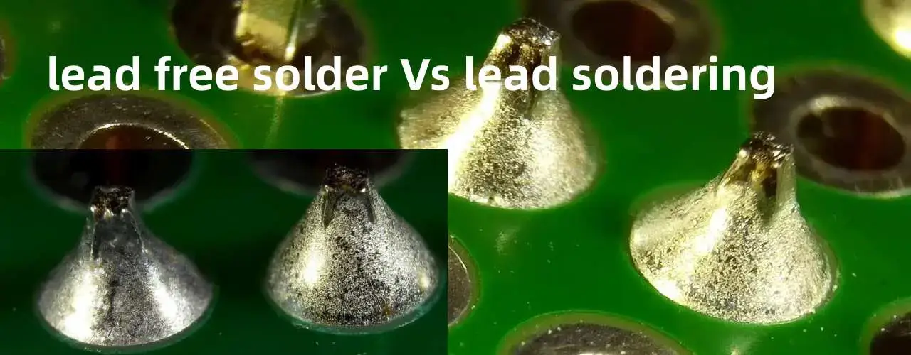
The decision to use lead-free solder affects more than procurement. The change in solder systems will impact solder compliance status, the ability to wet the component, and the amount of heat required for rework once the product has been assembled.
Why Process Temperature Changes
In the examples provided in the melting point comparison table, the largest difference between the melting points of the traditional tin-lead alloy solder and SAC305 lead-free solder is 30 degrees Celsius.
When Cost Changes The Decision
The process is more costly because of thermal process control, additional inspection, documentation, and compliance handling. If leaded solder is not legally or commercially possible, lead-free PCBA is the only option available, and comparing costs is secondary.
Solder Joint Inspection And Reliability Controls
Reliability of lead-free PCBA begins before the soldering operation and continues through final inspection. Each step in the inspection process has its own goal: confirming compatibility of materials, ensuring paste stability, verifying joint visibility, testing electrical continuity, validating powered characteristics, identifying long-term risk, and documenting any rework.
| Control item | Inspection focus | Record | Engineering risk |
|---|---|---|---|
| Material and BOM check | Lead-free solder, components, and PCB materials fit the required compliance and thermal process | RoHS / REACH compliant; SAC alloy record | Prevents a compliant solder choice from being undermined by nonmatching parts or finish. |
| Solder paste and placement check | Printing and component placement are stable before reflow | Solder paste printing; stencil design; component placement | Reduces bridging, insufficient solder, tombstoning, and wetting variation before reflow. |
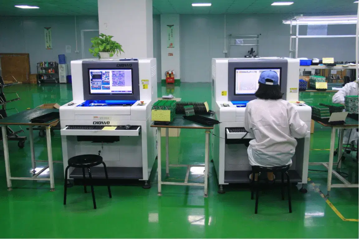
| AOI / SPI inspection | Visible solder, placement, and paste issues are screened | AOI; SPI | Screens paste volume, polarity, misalignment, bridging, and insufficient solder. |
| X-Ray inspection | Hidden solder joints and BGA / QFN / micro-BGA risks are checked | X-Ray | Supports void, hidden bridge, and under-package solder-joint review. |
| Wave / PTH solder control | Through-hole wetting, hole fill, bridging, and copper dissolution risks are controlled | Wave soldering; PTH assembly; 99.3 Sn/0.7 Cu | Separates PTH heat and wetting risk from the SMT reflow window. |
| Tin whisker risk control | Finish, alloy, storage, stress, and process records are reviewed | Tin whiskering; matte-tin and compressive-stress flags | Reduces long-term whisker risk through material, finish, coating, and process control. |
| ICT / FCT testing | Electrical connection and functional behavior are verified | 100% electrical test; ICT; FCT | Confirms circuit continuity and powered behavior after solder inspection. |
| Rework / desoldering control | Rework avoids pad, package, and laminate damage | Desoldering lead-free solder; higher thermal window | Controls heat exposure, flux use, pad condition, and acceptance record. |
| Final shipment check | Finished PCBA is checked before delivery movement | Testing and packaging | Protects the inspected assembly before shipment. |
BOM Material Check
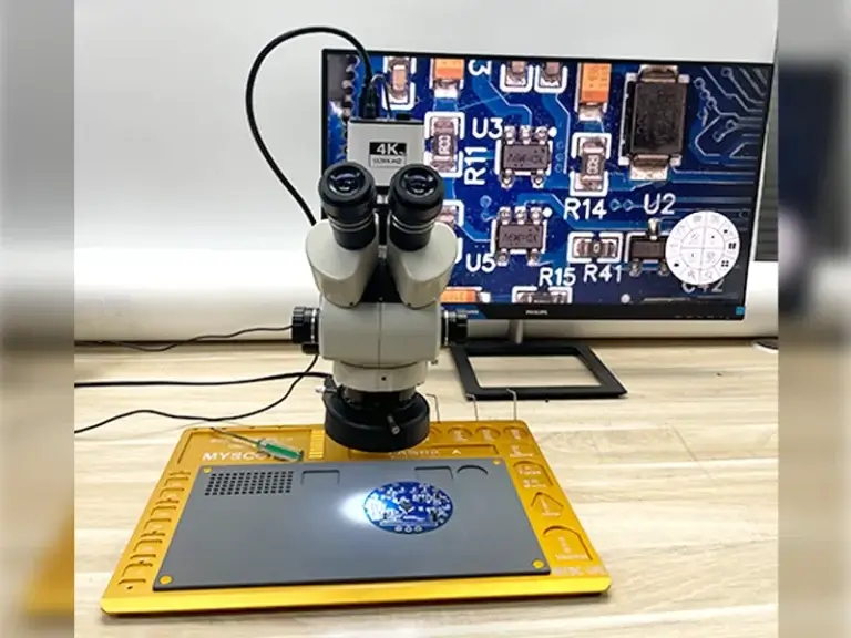
The first step in achieving lead-free reliability is identifying all of the components that will make up the BOM: component MPN, the status of the components, the PCB material, the MSL exposure, the surface finish of the PCB, and the solder alloy used in the assembly. The thermal exposure of high-Tg material may be an important factor if you are operating in a tight thermal tolerance application, and maintain the RoHS/REACH documentation for the components and solder.
Solder Joint Inspection
After the BOM has been identified, you have to choose your solder joint inspection method. Depending on how a joint will be inspected, how visible it is, and whether the paste was applied properly, you will choose different inspection methods to verify correct assembly. PTH and wave soldering will require different inspection considerations from SMT soldering: hole fill, bridging, non-wets, and copper dissolution are of significantly greater concern than appearance. For each manufactured PCB assembly, you will specify on the purchase order which class of acceptance you are adhering to. IPC-A-610J Class 2 / Class 3 and IPC J-STD-001J define the expected acceptance requirements.
Tin Whisker Risk
Tin whisker growth depends upon several factors: finish, alloy, storage conditions, mechanical stress, and soldering practices. Matte-tin finishes under the worst types of mechanical stress, such as press-fit connectors and plated mounting hardware, present the greatest risk of tin whiskering; conformal coating and post-plating annealing are two commonly used ways to mitigate the risk of tin whiskers for those applications. For electronics that require long service life, harsh environments, or are very sensitive to reliability issues, it is critical to ensure that the finish that is being used is appropriate for the soldering plan, inspection processes, and manufacturing records.
After-Soldering Electrical Checks
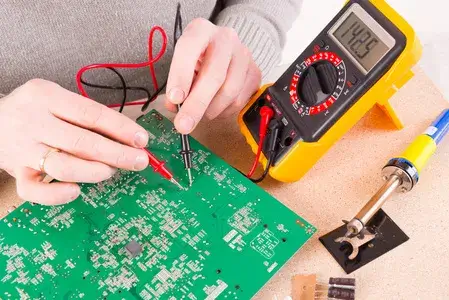
A post-solder inspection electrical test confirms that a circuit functions properly. Although a joint may look good under AOI, it may still fail continuity tests, load tests, or powered tests.
Rework is a documented exception to requirements. Desoldering lead-free solder will require more thermal process control. Controlling the heat applied, the flux used, the technician's process, the condition of the pads, and recording all of these factors protects the PCB from undue damage during rework.
Lead-Free PCB Assembly Applications
Lead-free PCB assembly is most commonly implemented when products need to comply with export rules, environmental requirements, user-contact safety requirements, long service life, or OEM customer compliance policies. Each application adds different stress to the components used, requiring different design and engineering considerations, as well as creating different causes of failure.

Automotive Electronics
Automotive control modules, braking electronics, infotainment systems, driver-assistance units, and sensor interface boards all require components and connectors that have achieved qualification to AEC-Q200 or equivalent, with connectors rated to withstand thermal cycling between −40°C and 125°C. The major lead-free-specific risk factors for automotive products deal with the potential for solder-joint fatigue caused by thermal cycling. Compared to leaded PCB assemblies, solder connections made with SAC305 solder are considerably stiffer, resulting in an increased risk of cracking at high cycle counts, particularly if the PCB assemblies will be subjected to significant vibratory loads. Consequently, X-ray or cross-section sampling is necessary to examine solder joints associated with BGA and connector attachments in vibration-heavy zones on automotive PCBs, whereas purely AOI methods will not provide adequate inspection of these solder connections. Additionally, connectors that are potted or conformal coated must also be verified for compatibility with no-clean solder flux residues prior to use. BGA and connector pads associated with vibration-heavy areas of PCB assembly should have an appropriately documented X-ray or cross-section sampling plan established prior to the first lot shipped for production, rather than waiting for a field return of the product to initiate the sampling plan.

Consumer IoT Electronics
Wearable technology, smart technology, gaming electronics, home-automation electronics, IoT gateways, Bluetooth devices, and LED lighting controllers all have similar packaging requirements, with a trend toward smaller BGA and QFN packages with increased moisture sensitivity ratings, MSL 2–3. In this application, the specific risks include improper baking and improper floor-life tracking. When a lead-free reflow profile is applied to components that have exceeded the specified moisture sensitivity limit, “popcorn” delamination can occur, and this is completely undetectable by AOI but can be identified through X-ray or acoustic microscopy. Other common points of failure in this category are coin-cell battery terminals and RF shield solder pads. Both connections require complete void-free wetting to meet contact-resistance and RF ground-return requirements. Because “popcorn” delamination is not typically seen until after completion of the reflow oven, the cumulative floor-life tracking of MSL 2–3 components should start at the time a reel is opened, rather than when it is placed on the pick-and-place machine.
Medical Device Electronics
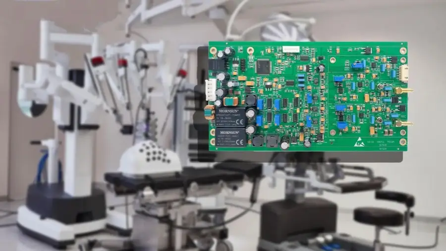
For medical device electronics, monitoring boards, portable device electronics, sensor modules, control electronics, and diagnostic interface boards will generally need to trace back to IEC 60601 electrical safety classifications. If the assembly supports a regulated medical device, the production records must also conform to ISO 13485 and have UDI-linked lot traceability. The primary concern regarding the risk of lead-free assemblies is less the solder alloy than the ability of the PCBA to reference and track all equivalent records, i.e., AOI, X-ray, ICT, and FCT, for each lot and UDI, so that the information can be cross-referenced with the PCBA device history file rather than residing in an independent, separate record set. Verifying a finished production lot’s UDI against the filed AOI, X-ray, ICT, and FCT results before shipping the production lot allows us to identify any missing documents that will create gaps in the device history files at a later time.

Industrial Control Boards
Industrial control boards are comprised of PLC I/O boards, motor-control boards, relay boards, terminal-block assemblies, power-control boards, and instrumentation-control boards, and all use both SMT and PTH methods in conjunction with mechanical vibration, electrical load cycling, and exposure to the surrounding environment. The recurring failure mode for these products is the thermal cycling of the high-mass PTH joint, also referred to as large-mass terminal block and connector solder joints, combined with the mechanical stress caused by vibration from being in a mechanical environment. Wave or selective soldering requires a longer dwell and higher pot temperature to completely fill the hole when joining these larger components together, and this dwell must be confirmed on the physical board, as opposed to assuming based on an SMT profile. Thermal mass and component type must be considered when sampling the thermal cycle fatigue of parts on the board. Terminal block joints have more thermal mass than all other components, thus the dwell time for terminal block joints must be longer than what would be used for SMT components, or the joint will be underfilled, even though the rest of the board will meet specifications.
LED Power Boards
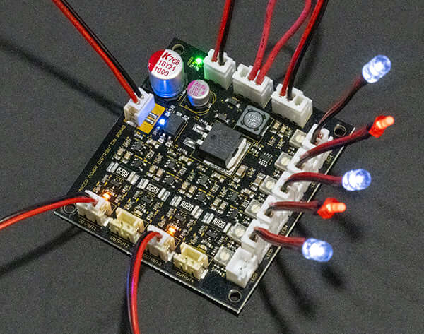
LED power boards are comprised of LED driver boards, LED lighting control boards, and LED high-power load control and power module boards, and these types of products have an additional source of continuous thermal cycling from power on and off switching, in addition to the lead-free solder question. A SAC305 joint in a high-current LED package on an MCPCB or heavy-copper board has a higher number of thermal fatigue cycles during its life than a standard signal joint does. Therefore, it is more important to evaluate the joint's reliability than simply how easily it can be soldered. The finish you select, whether lead-free HASL, OSP, or ENIG, must match your package pitch and the thermal mass of the PCB; for example, a finish that performs well with an FR-4 PCB may behave differently when it is used on an aluminum-backed MCPCB. To validate the reflow profile for an FR-4 prototype and an aluminum-backed MCPCB, you should test both by running the same reflow profile before finalizing your process. A reflow profile that fully wets the joint on an FR-4 may create a marginal joint on the aluminum-backed MCPCB because the heat sink dissipates thermal energy from the pad during reflow.

Harsh-Environment Electronics
Electronic devices deployed in harsh environments include aerospace-grade boards, defense electronics, robotics, energy equipment, oil and gas instrumentation, public sector municipal control systems, and communication modules. This category of products typically has a long service life and limited access for repairs — estimating the potential for a tin whisker failure due to the use of a matte tin finish on press-fit connectors and plated mounting hardware under compressive stress is among the most serious risks associated with harsh-environment electronics. Before specifying any conformal coating, the compatibility of the coating with the flux residue must be verified. Functional testing should include the full temperature and vibration envelopes rather than just room temperature before declaring these products acceptable. When the design includes press-fit connectors subjected to compressive stress, discussing the whisker risk with the finish supplier prior to the first prototype run is advisable since identifying the risk after completion of long-term testing often results in a requirement to requalify the joint whenever a coating change is made.
How To Choose A Lead-Free Assembly Supplier
Selecting a supplier for lead-free assembly should include evaluating the supplier's ability to maintain compliance documentation, soldering techniques, inspection, application requirements, separation of leaded and lead-free materials, testing, and packaging. It is best to assess the supplier based on actual records compiled from at least one real job rather than on their marketing capabilities.
| Supplier check | Engineering check | Evidence | SUGA capability |
|---|---|---|---|
| Compliance records | Match RoHS / REACH documents to solder, PCB finish, components, BOM, and PCBA lot | RoHS and REACH compliant; CoC / material declaration | Job-level compliance documentation tied to a specific lot. |
| Certification and standards | Confirm quality-system language and soldering acceptance criteria | ISO9001:2015 Certified; UL Listed; IPC-A-610J / J-STD-001J when specified | Quality-system and workmanship documentation on request. |
| Soldering coverage | Coordinate SMT, PTH, wave, reflow, selective, and manual soldering | SMT + PTH + manual assembly coverage | Full soldering-method coverage — detailed in the process table above. |
| Leaded / lead-free separation | Keep materials, tools, labels, and records identifiable | Leaded and lead-free PCB prototype control | Material and record control for separated builds. |
| Inspection methods | Select visible, hidden-joint, electrical, and functional checks | AOI, X-Ray, ICT, FCT | AOI, X-Ray, ICT, FCT, and electrical test options. |
| Board and order type | Support rigid, flexible, rigid-flex, prototype, small-batch, and high-volume builds | Rigid / flexible / rigid-flex; prototype / small-batch / high-volume | Rigid, flexible, and rigid-flex boards across prototype, small-batch, and high-volume orders. |
| Failure-mode match | Match experience to automotive, consumer / IoT, medical, industrial, LED / power, or harsh-environment boards | Application-specific failure-mode awareness | Process and inspection matched to board environment. |
Compliance And Certification Records
Compliance records are useful only when they are tied to the specific job — certifications such as ISO9001:2015 and UL, and workmanship standards such as IPC-A-610J / IPC J-STD-001J when specified, should be kept next to the production materials and final PCBA records from that job code. A compliance folder without a specific job number is paperwork, not supporting evidence; request that the supplier in question demonstrate actual evidence from a real job compliance package from beginning to end.
Process Capability
SUGA provides lead-free PCBA assemblies from PCB build through component procurement and assembly, to functional testing and delivery of the product across the full range of forms, including rigid, flexible, and rigid-flex boards, from short runs to large-volume builds. This coverage extends to turnkey, partial-consignment, and consigned assembly, as long as clear material and process controls are maintained as the order moves from prototype to repeat build.
How Are Leaded Builds Kept Separate?
SUGA can provide both leaded and lead-free PCB prototypes with clearly separated solder identities: clear identification of materials, work instructions, labels, and traveler records provides the ability to identify the build condition before actual production begins. This is especially critical when working on a legacy project and a RoHS-compliant project through the same production flow at the same time.
Reliability Records
Reliability records should be matched to the risks that the PCB boards carry — a solder joint that is visually acceptable under AOI inspection is not sufficient if there is a need for powered or electrical verification that the board functions correctly. IPC-A-610J and IPC J-STD-001J align acceptance criteria and expectations for soldered joints with the soldering process referenced in the purchase order. SUGA links solder-joint and soldering-process expectations to the actual material, soldering, and testing conditions of the product.
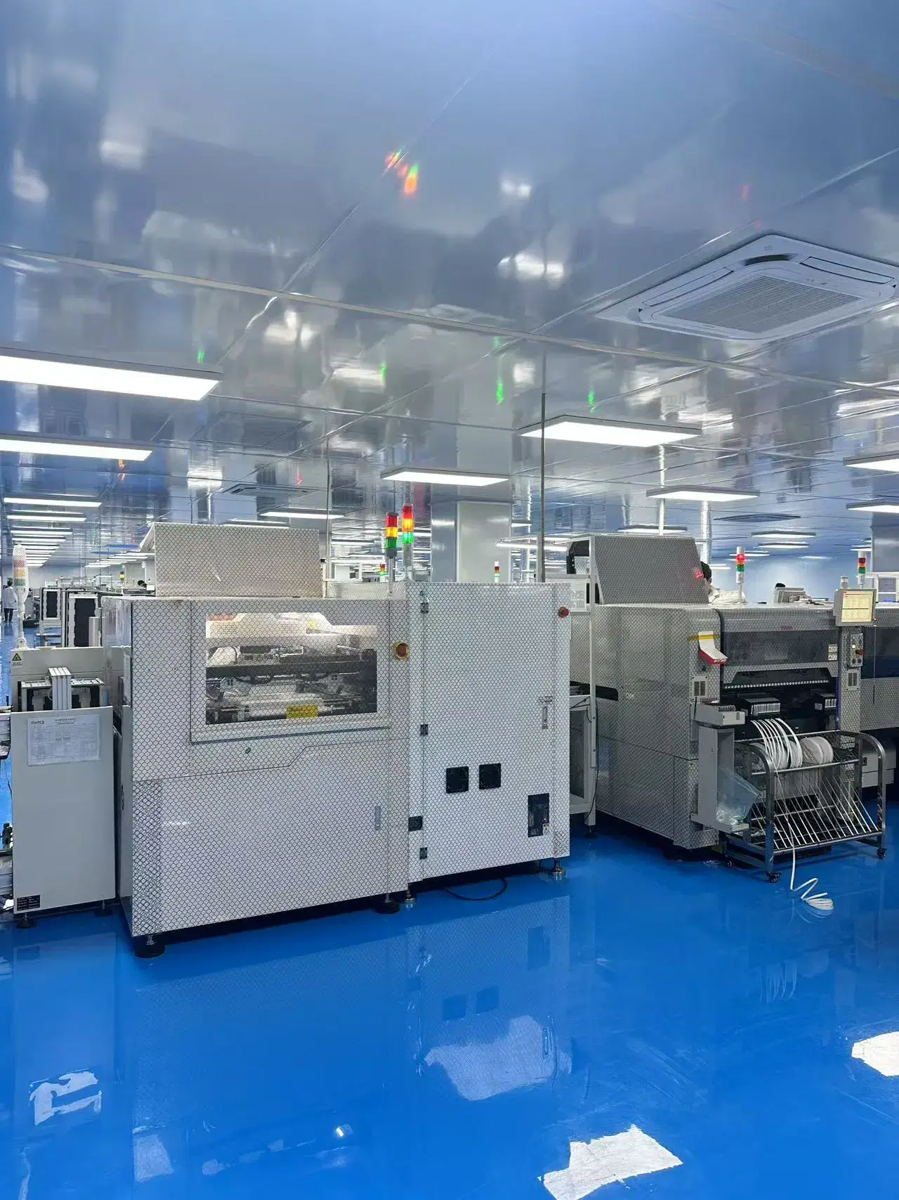
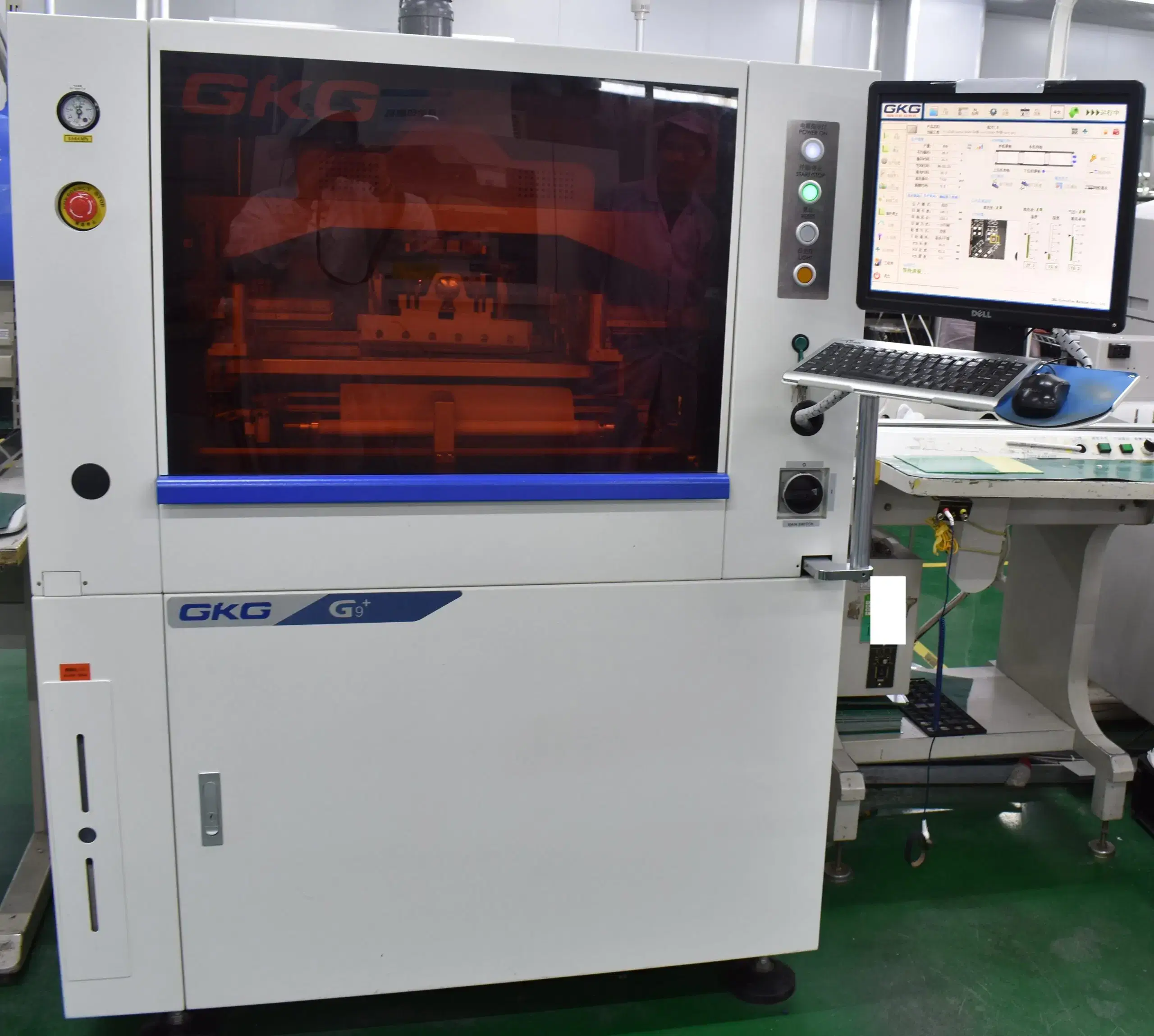
Our PCB Factory Gallery
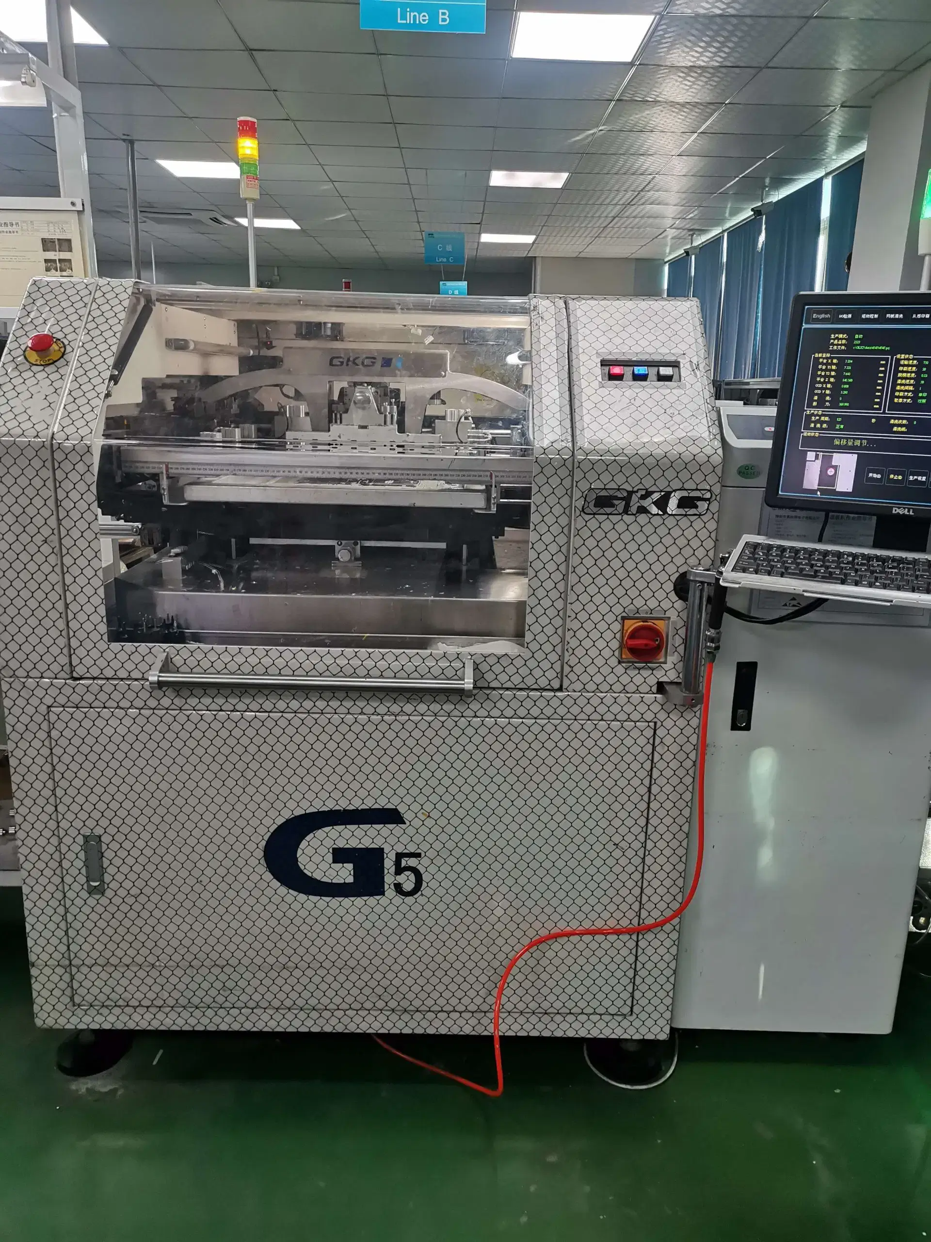
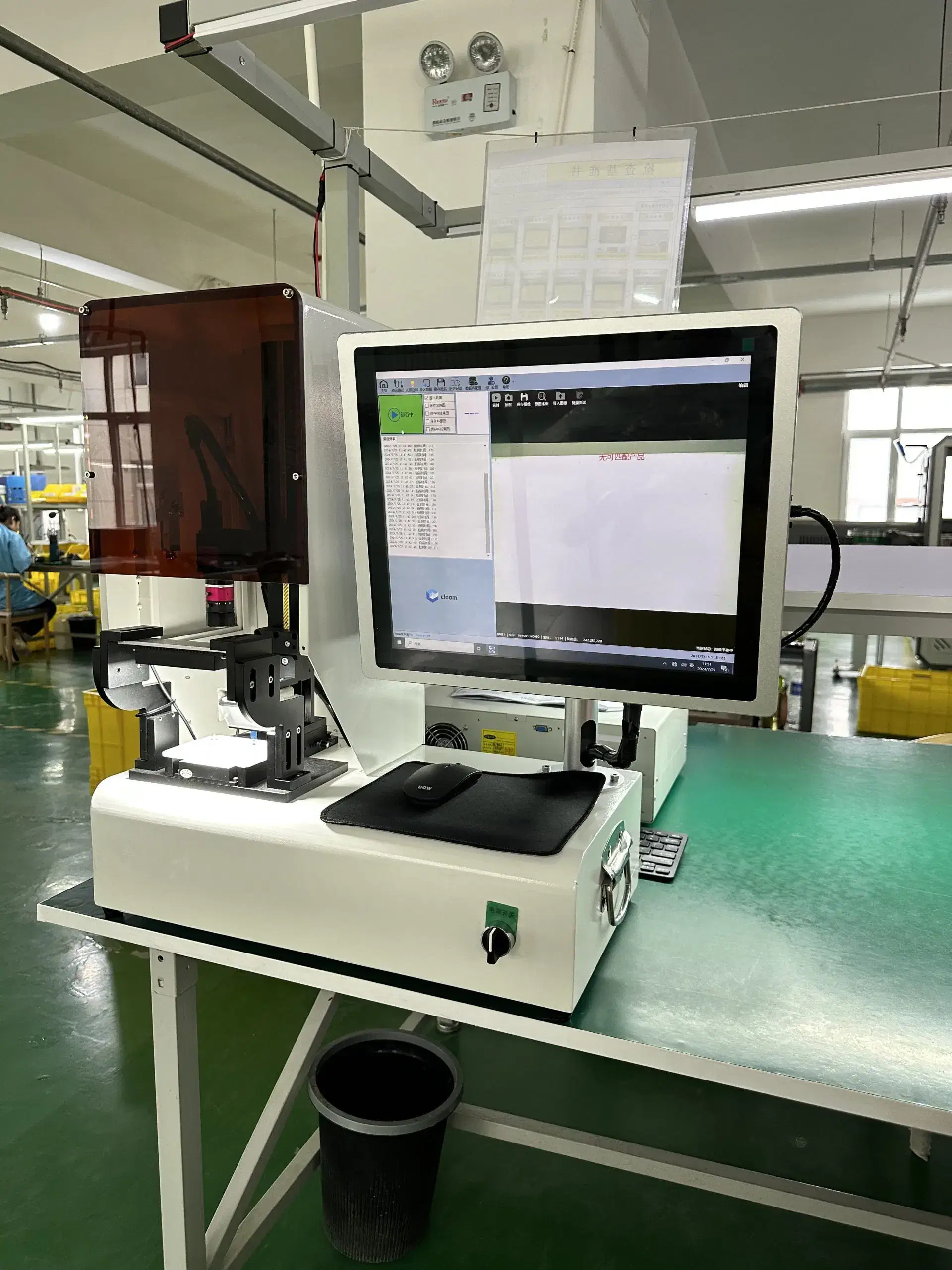
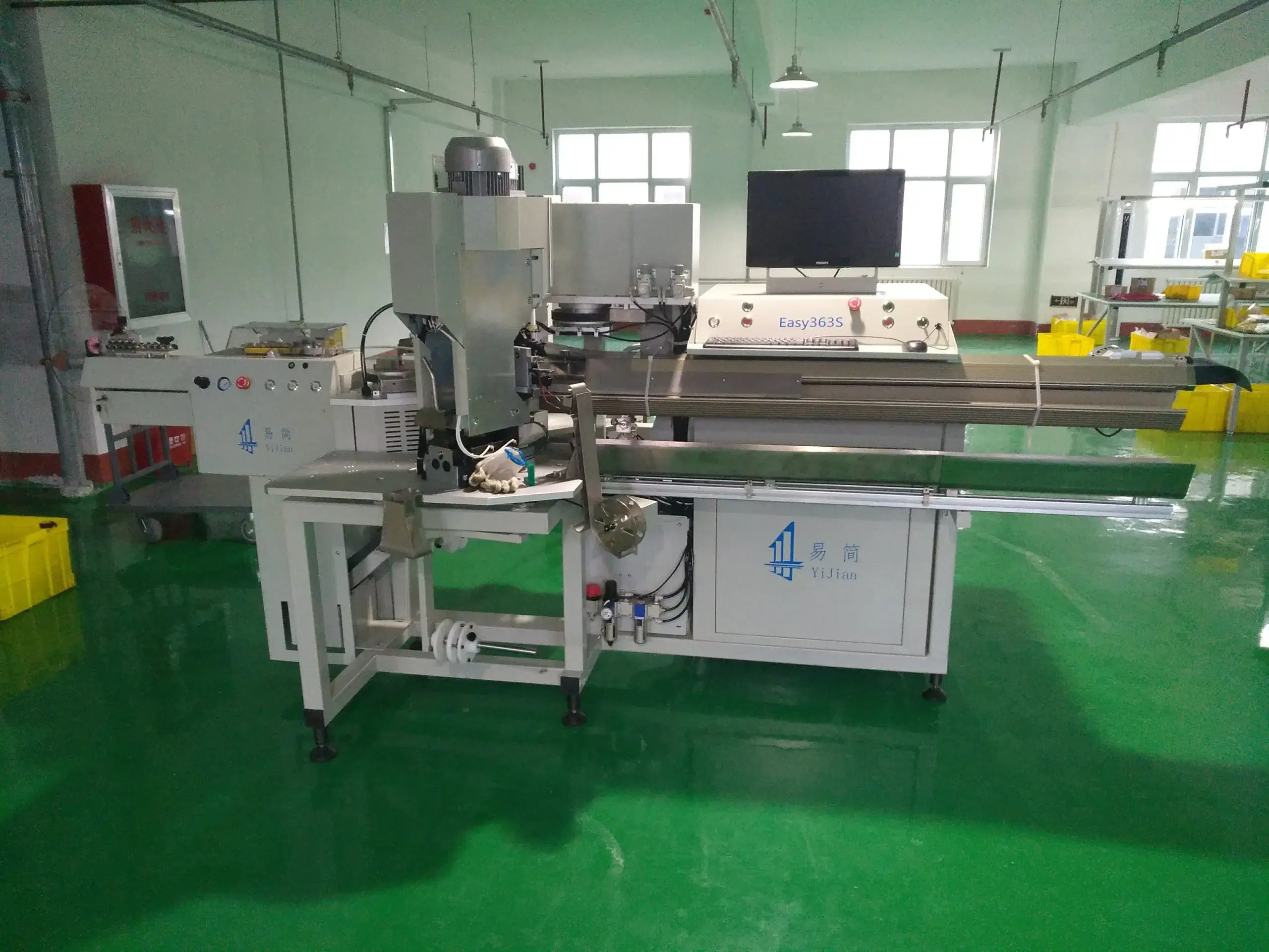
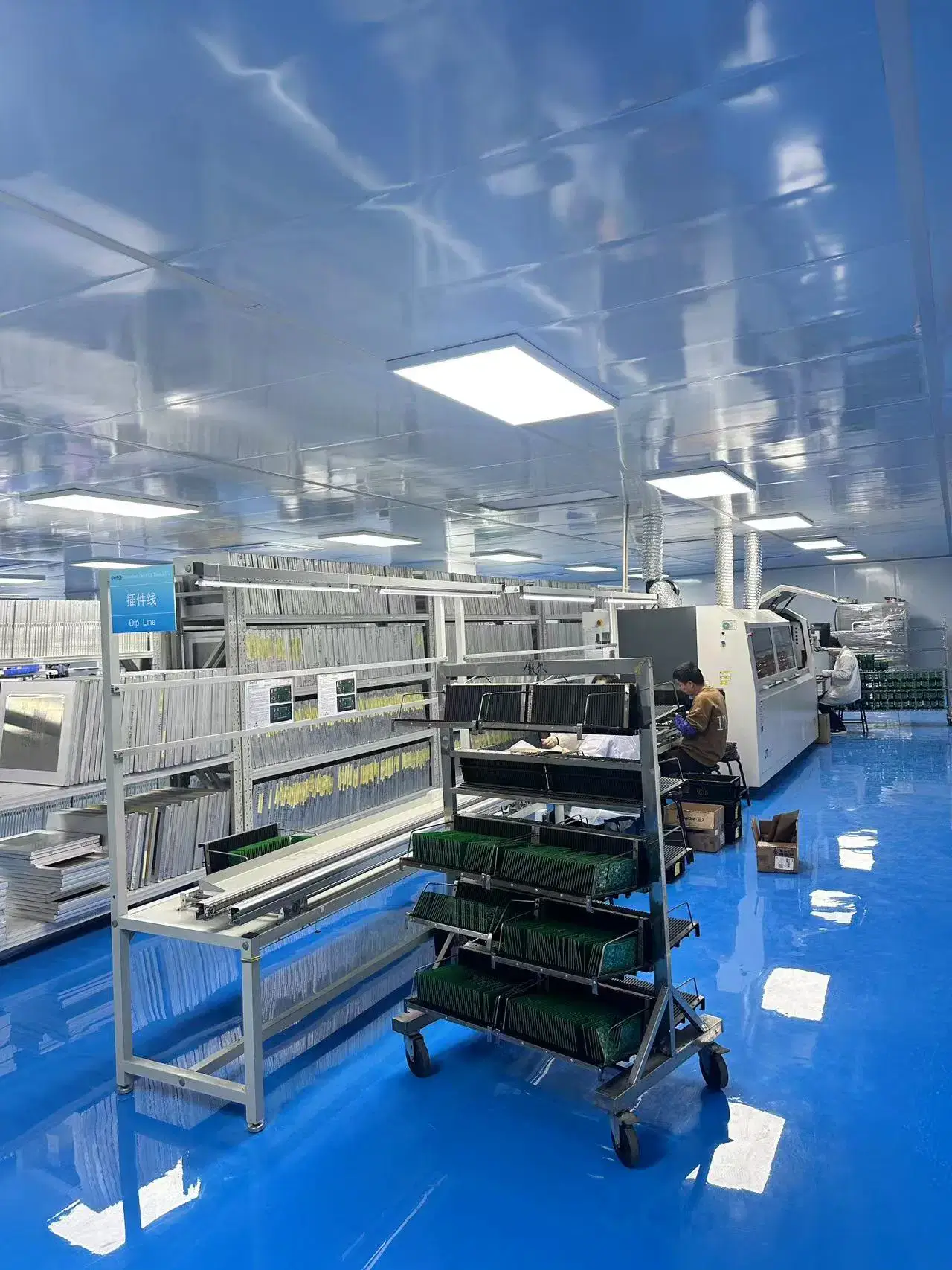
Frequently Asked Questions
A lead-free PCB assembly is the assembly of a PCB using lead-free solder materials and controlled SMT, PTH, reflow, wave, selective, and manual soldering with compliance records and an overall inspection to produce RoHS-compliant PCBA.
Lead-free solder is a solder alloy with no lead as a predominant soldering metal. The most common lead-free solder for SMT reflow is SAC305.
Lead-free solder means that the solder meets the RoHS restricted-substance limits for solder and finished PCBA. This does not mean that there is no lead; trace lead can come from plating, components, or alloy impurities, but still be below the limit and meet the criteria for RoHS.
RoHS restricts the following ten substances: lead, cadmium, mercury, hexavalent chromium, PBB, PBDE, and the four phthalates (DEHP, BBP, DBP, DIBP). In most cases, sourcing and processing teams focus on lead and cadmium because of the compliance limits used to determine if lead and cadmium exist. For lead, the limit is 1000 ppm and for cadmium, it is 100 ppm.
SAC305 (96.5% Tin, 3% Silver, 0.5% Copper), which melts at around 217–220°C, is a common lead-free solder for use in SMT reflow applications. SnCu (99.3% Tin, 0.7% Copper) is also found in wave soldering and solder wire.
The temperature required for lead-free soldering is higher than that of leaded soldering, depending on what method is being used. Wave and selective solder pot temperature is between 250–280°C. Reflow generally has a peak temperature of approximately 240–260°C for SAC alloys, with the specific temperature requirement determined by board mass, component limits, paste, and finish.
In PCB assembly, RoHS verification is documented within the solder and materials limits referenced above. REACH documentation contains the SVHC declaration and is available alongside RoHS verification. Both RoHS and REACH documentation must be filed on the same BOM revision so that customers conducting audits can locate documentation for either verification without requiring cross-reference between two documents.
Yes, lead-free solder is more suitable than leaded solder for RoHS compliance, export, and environmentally regulated electronics products. Leaded solder is only acceptable for products where lead is explicitly allowed.
Yes, lead-free solder is acceptable for electronic use. For best results, the lead-free solder materials used must be compatible with the electronic assembly in regard to the alloy, flux, temperature profile, and inspection methods.
The additional expense associated with lead-free solder materials results from the cost of the alloy metals, thermal process control, inspection, documentation, and compliance handling, which is higher than for leaded assembly.
Lead-free solder joints may develop problems such as bridging, voids, non-wets, too little solder, tin whisker risk, pad lift, and rework stress when the process controls are ineffective. The risk of tin whisker formation is concentrated in matte-tin finishes when these finishes are placed under compressive stress, such as in press-fit connector applications.
Yes, SUGA offers both assembly options, utilizing dedicated materials, tools, solder alloys, labels, traveler records, and manufacturing records to ensure that legacy builds and RoHS-compliant builds are identifiable.
Yes, SUGA provides lead-free PCB assembly services for SMT, PTH, wave soldering, reflow soldering, selective soldering, and manual soldering. SUGA also provides RoHS and REACH documentation for assembled printed circuit boards as well as the inspection and test methods described above for finished products.