Upload BOM & Gerber
-
Mobile: +86 13312967631
-
Email: sales@sugaintl.com

Consigned PCB Assembly Services
Consigned PCB Assembly Supplier in China for Controlled Production Using Customer-Supplied Components
Keep control of approved, proprietary, allocated, or pre-purchased parts while SUGA manages incoming checks, kitting, SMT and through-hole assembly, inspection, testing, traceability, and residual inventory reporting.
01005 placement; machine placement accuracy within ±40 μm; BGA ball diameter/pitch down to 0.20 mm/0.35 mm.
AOI, X-ray, ICT and FCT; workmanship and soldering controls aligned to IPC-A-610J and IPC J-STD-001J when specified.
What Is Consigned PCB Assembly?
Consigned PCB assembly is a contractual manufacturing agreement in which the customer provides most or all of the materials necessary for the finished product, and SUGA warehouses, inspects, kits, assembles, solders, tests, and returns the finished product to the customer. SUGA takes controlled custody of the customer-supplied materials upon receipt and acceptance. In addition to maintaining custody of the supplied materials, SUGA also takes responsibility for the assembly process once the supplied materials have been accepted.
A consigned part is more than just a single component shipped from the customer to an assembler. A consigned part requires the identification, counting, packaging, labeling, lot numbering, and revision identification of all parts associated with the board in which the consigned part will be used. Consequently, ownership, custody, and production responsibility must be separated into three distinct categories and cannot be determined simply by the description, “you supply it, we build it.”
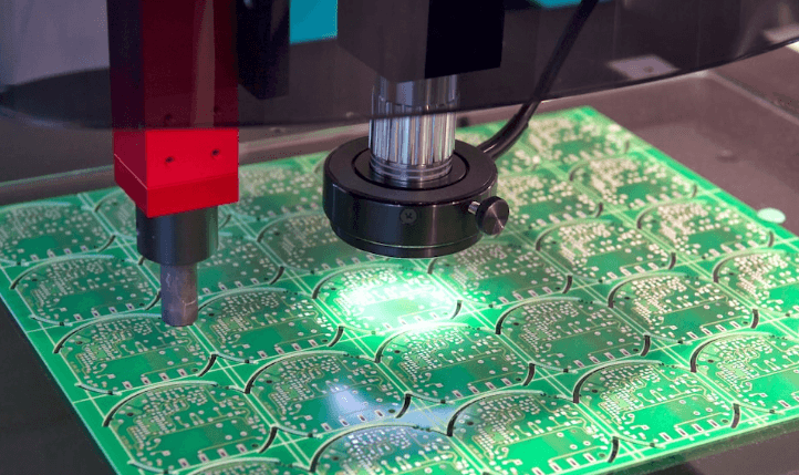
| Responsibility area | Customer role | SUGA role | Production impact |
|---|---|---|---|
| Component ownership | Owns all or selected consigned parts | Maintains custody and controlled use after acceptance | Ownership does not remove the need for receiving records and quantity reconciliation |
| Material identification | Supplies BOM-matched part number, value, and PCB designator labels | Verifies labels, packaging, and quantities against production data | A mismatch halts the affected line item before placement |
| Procurement | Supplies all parts in full consignment or selected critical parts in partial consignment | Sources only the agreed balance of parts in partial consignment | Procurement risk follows the party responsible for each BOM line |
| Assembly | Supplies approved components and applicable product data | Completes kitting, placement, soldering, inspection, and testing | Manufacturing responsibility begins upon acceptance of the kit |
| Residual inventory | Retains ownership of the remaining material | Counts, stores, and reports the remaining material by an agreed identifier | Repeat orders rely on accurate residual inventory records |
Who Owns and Supplies the Parts?
Full and partial consignment differ in the volume of BOM material supplied by the customer, not in the way SUGA treats the material once it has been accepted. Full consignment applies when inventory already exists in the customer’s possession, including proprietary devices, controlled lots, and parts sourced from an approved source; therefore, the origin of every line item must be known. Partial consignment is used when only designated high-risk or allocated parts require the same level of control.
Each BOM line needs a single responsible party. This ensures that a passive item is not purchased more than once and that any missing semiconductor is identified as belonging to the correct responsible party rather than being assumed to belong to another party. Before any material is released for production, labels must match the BOM part number, part value, and PCB designator.
Receiving indicates that SUGA has accepted custody of the material, but accepting custody does not mean that SUGA owns it. Once the material has been accepted, it passes through kitting, placement, soldering, inspection, testing, and reconciliation of the remaining material balance.
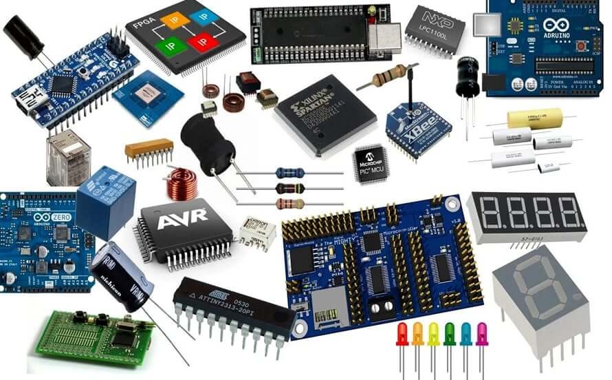
Turnkey vs. Consigned PCB Assembly
Turnkey PCB assembly differs from consigned PCB assembly based on ownership of the BOM lines.
When Full Consignment Is Appropriate
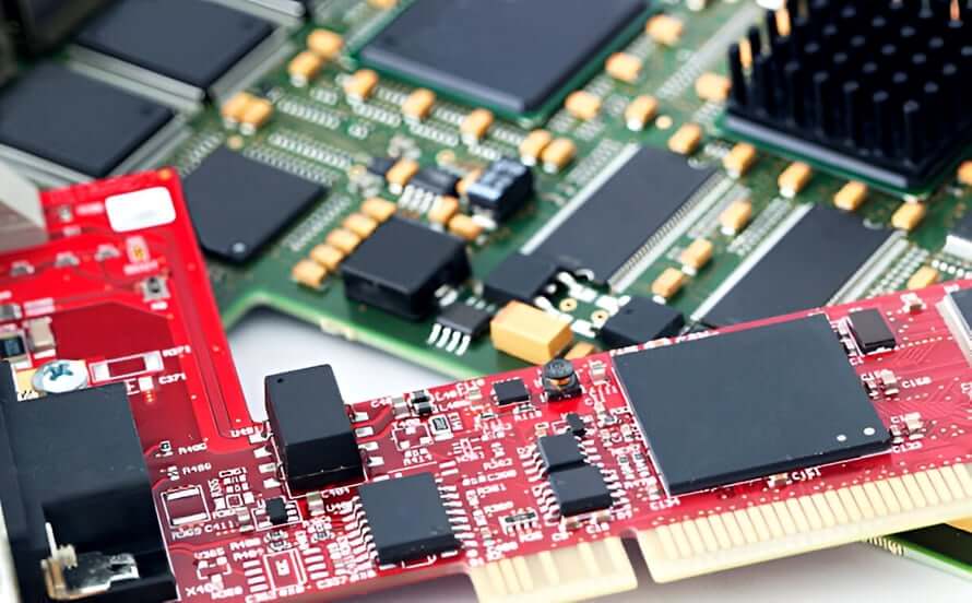
When the need for material control is greater than the need for outsourced procurement, full consignment is appropriate. Examples of situations that trigger full consignment include previously purchased inventory, proprietary devices, allocation-constrained components, a predetermined AVL or AML, and customer-controlled lot identity. Full consignment also allows customers to use excess stock without giving up its source history.
When controlling the parts, the customer also controls the risk of their availability. To initiate assembly, a complete kit, correct labeling, usable packaging, and sufficient quantities must be supplied to SUGA. Once accepted, SUGA is responsible for process discipline and providing the required quality records.
Partial Consignment
Customers often use partial consignment by retaining an allocated processor, approved memory, or programmed device while SUGA sources standard passives and other items. Retaining only the highest-risk components under customer control helps customers avoid the added burden of consigning all low-risk components.
BOM reconciliation provides an audit trail that identifies who supplied every BOM line, prevents duplicate purchases, and makes substitution authority explicit. Thus, the customer-supplied kit and the sourced balance remain under one production plan during assembly.
Turnkey Assembly
Turnkey assembly is a good option for customers whose BOMs are stable and who do not wish to manage multiple purchase orders, incoming shipments, or individual material availability.
Without written purchasing agreements that define sourcing, lot, and pricing controls, such as an approved vendor list, designated manufacturers, lot traceability, or open-book BOM pricing, turnkey assembly gives customers less direct control over individual procurement transactions. This is a disadvantage when a project uses proprietary devices or fixed vendor requirements without those controls in place.
The planned lead time for procurement and assembly of components with normal availability is typically 10–15 days. Constrained or custom-sourced components require dedicated scheduling.
How Are Customer-Supplied Parts Controlled?
At the start of a consignment PCB assembly control procedure, received materials (parts) are matched to the corresponding BOM and placement data. Before line setup, SUGA verifies the identity, quantity, packaging, condition, lot/date codes, and revisions of incoming materials. All mismatches will be isolated as early as possible to prevent a material issue from becoming an assembly defect.
Incoming Material Verification
While verifying the identity of incoming materials, physical labels from the manufacturer, manufacturer part numbers, and packaging types are compared with the BOM before checking the quantities and visible condition of incoming parts. A correct quantity of parts with the wrong identity will still fail receipt. Customer-supplied PCBs will be subject to the same verification process; the verification consists of confirming the identity, revision, panel format, quantity, and surface condition of the customer-supplied PCB against the assembly data.
Shortages, identity mismatches, damaged packaging, and uncertain revisions are segregated under their original identifiers until resolved.
Kitting and Shortage Control
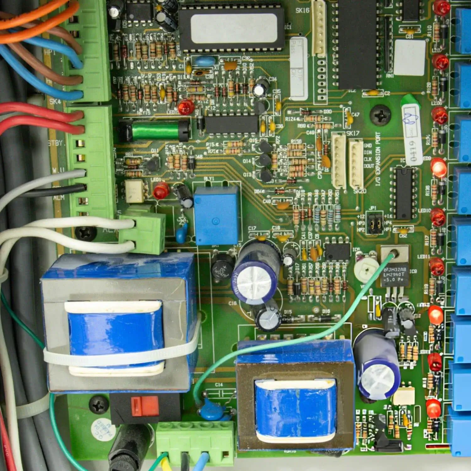
Kitting is the process of taking accepted materials (parts) and turning them into a feeder-ready or insertion-ready kit. Bins, reels, cut tape, trays, and tubes remain associated with their part and lot identifiers while operators count and prepare them. An incomplete reel may be usable, but leader length, damaged pockets, mixed lots, or uncertain quantities can cause a change in the preparation method for these partial reels.
The shortage report includes the affected BOM line and the usable amount remaining. All excess materials remain associated with their original identifiers to protect the upcoming production lot from unnecessary recounts.
Moisture and Static Protection
Moisture-sensitive component control is established using exposure history and not the label alone. The integrity of the packaging, humidity indication, and the storage and handling history of components may determine whether a device can move through the manufacturing process as intended, requires controlled storage, or needs approved exposure recovery or baking. A dry cabinet that maintains ≤10% RH may provide one possible storage condition, but it does not replace the MSL rules for the components.
ESD protection continues through storage, kitting, and line transfer.
Material Identity Before Kitting
Prior to kitting, the BOM revision, placement data, lot/date code, and reel ID must all indicate the same production intent before the material reaches a feeder. Old-revision material cannot be added to a new-revision setup based on assumption. There must be an approved disposition for these items.
This pre-production link differs from final traceability. The objective of this link is to prevent the wrong material or revision from entering the line. Installed quantities, test records, and scrap will be reconciled later after the assembly process has been completed.
Consigned PCB Assembly Process
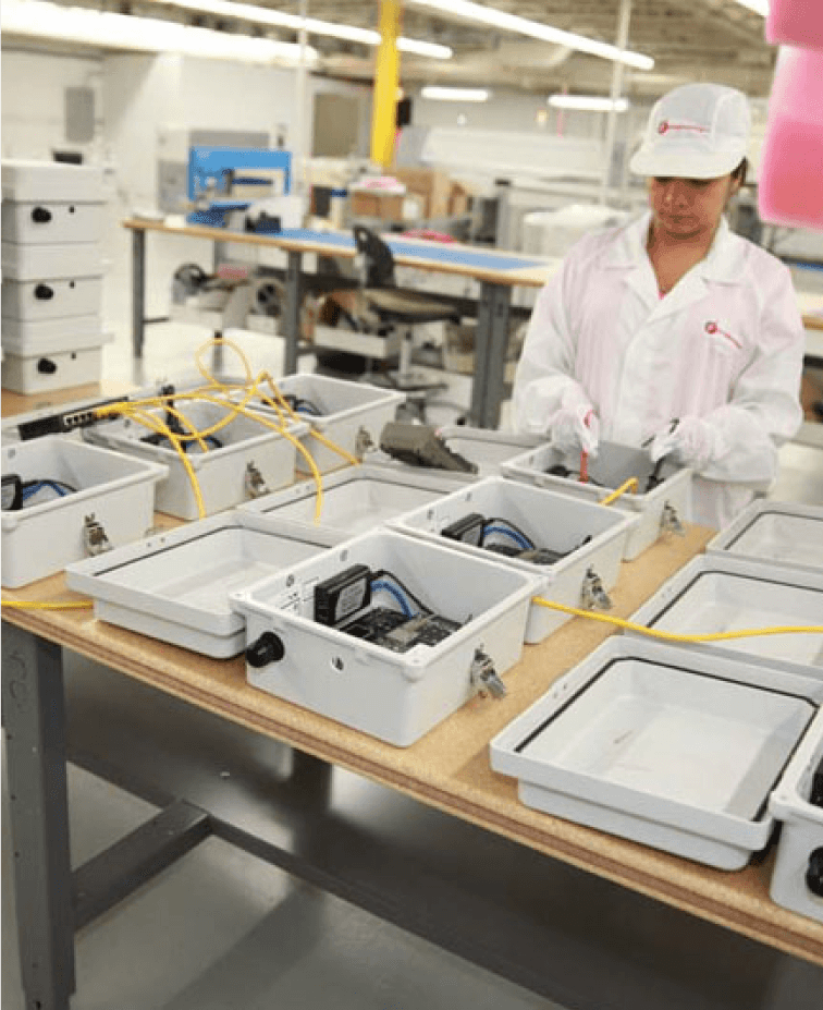
As soon as SUGA has accepted the customer-supplied materials and production data, the consigned PCBA process will proceed through eight stages of manufacturing.
- Engineering check: The engineering process aligns the BOM, placement data, board data, component identities, polarity, and assembly method. If there are conflicting data sets, the process stops.
- Incoming material acceptance: Check the identity, quantity, packaging, and condition of the incoming materials according to the SUGA specification for customer-supplied PCBs and components.
- Stencil and line preparation: Establish solder-paste conditions, feeders, support, and profiles based on the package mix accepted into production.
- SMT placement: Place feeder-ready components under program, polarity, fiducial, and first-article controls.
- Soldering: Use reflow, wave, selective, or controlled hand soldering processes based on the type of assembly produced.
- Inspection: Apply visual, AOI, and X-ray inspection as required by the package geometry and potential defect risk.
- Electrical testing and FCT: Test using the agreed open/short, ICT, or FCT method and record the disposition.
- Final records and inventory reconciliation: The final assembly records will note quantities, traceability, and any remaining customer-owned stock.
Production Data Alignment
The engineering check compares the material and production data to verify that they match the board being manufactured. Prior to setting up the production line, SUGA assures that revisions, package identifiers, polarity, placement coordinates, and soldering order are all in sync. Mismatched QFN package types, reversed polarity definitions, or obsolete placement files must be corrected at this stage.
The geometry of the components will be used to determine the inspection method for each component. BGAs and QFNs may require X-ray inspection, but a mixed combination of SMT and THT may require multiple soldering operations.
Preparing the SMT Line
As a fine-pitch engineering example, a 100 µm foil thickness would correspond to a 0.5 mm pitch, while an 80 µm foil thickness corresponds to a pitch of 0.3 mm or smaller. Characteristics such as area ratio, package mix, type of paste used, whether a stepped stencil is required, and the transfer balance of the board will influence the final decision on which stencil is used.
Placement controls incorporate the capabilities of the machines with the placement fiducials on the boards, board support, package geometry, and first-article documentation.
Mixed-Technology Soldering Sequence
Typically, SMT components are reflowed, but mixed assemblies may require multiple soldering processes.
Factors such as component height, thermal mass, side selection, previous exposure to heat, and protection of components already attached to the first side will determine the order in which the soldering processes are executed. Support tooling and connector geometry influence side selection as well. Inspection and test documentation may be obtained at various stages during the soldering operations instead of only at the completion of the entire soldering operation.
Our Assembly Capabilities
| Capability | SUGA Capability | What it proves | What to Confirm |
|---|---|---|---|
| Nominal placement throughput | Up to 60,000 components per hour | Available machine capacity for dense SMT population | Compare nominal CPH with feeder changes, first-article checks, placement count, lot size and line balance; it is not the same as completed-board output |
| Machine placement accuracy | Within ±40 μm | Positioning capability for fine-pitch packages | Match the machine specification to package pitch, pad geometry, board fiducials, warpage and the inspection method |
| Small passive placement | Down to 01005, approximately 0.4 mm × 0.2 mm | Capability for miniature passive placement | Confirm component packaging, feeder availability, stencil aperture, board finish, rework access and inspection resolution |
| QFN geometry | Terminal width down to 0.15 mm and terminal pitch down to 0.25 mm | Fine-pitch bottom-terminated package capability | Pair with paste-transfer control, thermal-pad design, profile development and X-ray acceptance criteria |
| BGA geometry | Ball diameter down to 0.20 mm and ball pitch down to 0.35 mm | Dense area-array placement capability | Pair with PCB escape design, profile control, X-ray criteria, rework strategy and package-specific engineering review |
| Panel and board envelope | Up to 520 mm × 400 mm; board thickness 0.6 mm to 3.2 mm | Physical transport and handling range | Check panel rails, component keep-outs, board support, warpage, mass and machine transport limits |
| Assembly methods | SMT, PTH/THT, mixed-technology and double-sided assembly; DIP, SOP, SOT, QFP, QFN, BGA and µBGA | Coverage across common package and soldering methods | Map every BOM package to placement, insertion, soldering, cleaning, inspection and rework access |
| Inspection and test methods | Visual inspection, AOI, X-ray, open/short testing, ICT and FCT | Evidence layers from visible workmanship to connectivity and intended operation | Select methods according to hidden joints, defect risk, test-point access, fixture availability, customer test specification and lot traceability |

Through-Hole Assembly
Through-hole assemblies use electrical or electronic connection devices such as connectors, transformers, relays, switches, power components, or similar types of components where insertion and an appropriate soldering method are necessary. For through-hole assemblies, lead-forming methods, required insertion depths, and clinching operations influence the consistency of the assembly process prior to soldering.
The nature and amount of copper present and the thermal mass of the assembly have an important bearing on the selection of wave, selective, or controlled manual soldering processes used in PCB assembly. Furthermore, whether solder fills the hole completely, whether the top side has received sufficient wetting, assembly cleanliness, the amount of mechanical load applied during the assembly process, and ease of access for inspection are also significant considerations when selecting a soldering method for through-hole components.
How Is the Assembly Process Selected?
These capabilities define the limits of the available assembly methods. The materials defined by the design’s BOM and confirmation of the accepted material conditions determine which of these methods will apply to any specific assembly. For example, if a design incorporates a BGA with a pitch approaching the minimum specification, is a mixture of SMT and THT, and requires FCT approval by the customer, then multiple capabilities would apply to that assembly simultaneously, and each capability would contribute to the lead time required for that design’s first article and corresponding fixture.
When a BOM approaches the specified assembly limit, SUGA will flag that item for a more complete engineering review prior to defining the assembly lead time, rather than assuming that the nominal assembly capability applies to that BOM.
PCB Fabrication Compatibility
In cases where PCB fabrication is included in the process, the bare-board construction must accommodate the assembly process. Bare-board construction parameters that determine the ability of the completed bare board to support the design and allow soldering, handling, inspection, and production yield include layer count, trace/space ratio, and related construction factors. Combining fabrication and assembly reviews prior to placement, reflow, through-hole soldering, or testing minimizes the chance of a fabricable bare board becoming unstable during assembly.
| PCB fabrication capability | SUGA Capability | Assembly relevance | What to Confirm |
|---|---|---|---|
| High-layer-count PCB | Up to 64 layers | Supports combined PCB fabrication and assembly projects that require high-layer-count construction | Confirm stack-up, material availability, registration, via structure, copper distribution, impedance, test method and assembly thermal exposure |
| Fine trace/space | Down to 1.8 mil / 1.8 mil | Supports dense interconnect designs when PCB fabrication is included | Verify copper weight, finished copper, etching tolerance, impedance needs, via structure, yield and panel utilization |
| RF and high-frequency boards | Designs operating up to 60 GHz | Supports combined PCB fabrication and assembly planning for specified high-frequency designs | Confirm laminate system, Dk/Df control, insertion-loss target, copper profile, impedance coupon, connector launch and the customer-defined RF test method |
| Assembly compatibility review | Fabrication and assembly requirements are reviewed together | Connects board construction to soldering, handling and inspection requirements | Check surface finish, pad geometry, warpage, copper balance, thermal mass, solder-mask definition and package-specific assembly limits |
How Are Quality and Traceability Verified?
For quality records to be credible, they must link the accepted material identity to an assembly lot or serial number, apply the specified workmanship criteria, document inspection and repair dispositions, and trace electrical or FCT results to final acceptance. A certificate logo does not prove the quality of any single PCBA lot.
RoHS or other market requirements should be treated as project evidence and not as a substitute for material records or product assessment.
Which Standards Apply?
ISO 9001:2015/Amd 1:2024 is a QMS standard; ISO 13485:2016 covers QMS for medical devices; and IATF 16949:2016 applies to an eligible automotive manufacturing scope.
IPC-A-610J provides information on the acceptability of electronic assemblies, whereas IPC J-STD-001J provides information on soldering materials, processes, and requirements. The product requirement defined by the customer determines which IPC class applies, including Class 2 or Class 3 when specified. IPC/JEDEC J-STD-033 provides information specific to moisture/reflow-sensitive device handling; ANSI/ESD S20.20-2021 concerns the establishment of an ESD control program; and IPC-7711/7721D provides controlled rework, modification, and repair methods.
How Is Each Material Lot Linked to Finished Boards?
Traceability allows customer-owned materials to be tracked throughout placement, inspection, testing, and material closure. Each accepted lot ID or container ID is connected to the assembly lot or serialized unit and maintains a record of installed quantity, verified scrap, and remaining quantity.
The material balance is stated in explicit terms: received quantity minus installed quantity minus verified scrap equals residual quantity, subject to recorded returns or approved adjustments. This residual stock is given one of three outcomes: SUGA will return it, store it under controlled conditions, or transfer it to the next approved lot. All outcomes maintain the identifier, quantity, condition, and revision status.
Evidence Across the Assembly Lot
There is no single method that verifies workmanship, connectivity, and function. Bare-board electrical testing is only applicable where PCB fabrication has been included.
| Verification need | Verification type | What it can establish | Important limit |
|---|---|---|---|
| Missing, shifted, reversed or visibly mis-soldered component | Visual inspection and AOI | Visible placement, polarity, marking and solder-feature conditions | Cannot fully evaluate hidden BGA/QFN joints or prove intended circuit operation |
| Hidden BGA, µBGA or QFN solder condition | X-ray | Hidden-joint alignment, void indicators, bridging, opens or insufficient solder signatures subject to the inspection method | Does not by itself prove electrical function or all metallurgical reliability conditions |
| Open or short connectivity | Open/short test or ICT | Connectivity and selected circuit-node results | Coverage depends on test access, netlist, fixture and program design |
| Component value, orientation or selected powered node | ICT where access exists | Installed-value, polarity and selected node measurements | Cannot replace full product operation or system-level behaviour |
| Intended board operation | Customer-defined FCT | Agreed power-up, interface, signal or functional behaviour | Proves only the functions, limits and conditions included in the approved test specification |
| Repair or material exception | Disposition and rework record | Reason, action, operator/process trace and re-inspection result | A record must remain linked to the affected lot or serial number to support traceability |
How Order Volume Affects Turnaround Time
Shipments do not initiate the assembly time until the assembly kit and production data are fully evaluated and approved. Instead, many variables may affect the schedule once the kit and production data are approved. For instance, incomplete shipment information, missing line items in the BOM, uncertainty about custom fixture requirements, complex assembly such as fine-pitch SMT, testing and validation requirements, and potential repair needs will affect the schedule.
What Drives Turnaround Time?
If there is missing or conflicting information on the BOM, then that will alter the timeframe for assembly. Revisions cannot be closed until the parts, test method, inspection technique, and machine program accurately describe the same assembly that was ordered.
Assuming a complete and accurate kit, reliable and stable production data, standard assembly processes, and the absence of any custom fixture requirements, the typical turnaround time for assembly-only work is about five working days.
The preparation and first-article work performed will depend heavily on the complexity of both the package and board. Functional fixtures will normally require more engineering time compared with basic assembly-only requirements. Although line capacity will affect turnaround times, an incomplete kit cannot be resolved by line capacity.
Test-fixture design, customer-specific software, calibration testing, environmental screening, and system-level validation activities fall outside the normal timing for basic assembly unless specified within the scope of work.
Prototype and NPI Runs
The typical timeframe for prototype or NPI lots is 2–4 working days, depending on several factors such as material completeness, revision closure, PCB complexity, stencil status, requested testing, and first-article scope.
Although prototype and NPI lots are typically used to test circuit function, they also identify gaps in material identification, machine program issues, solder profile requirements, inspection coverage, and test point availability. First-article records protect the remaining components in the kit by documenting the chosen inspection method for use within compressed timeframes. The machine program can be reused for future lots once it has been established and stabilized.
Repeat Low-to-Medium-Volume Production
For repeat low-to-medium-volume PCB assembly after kit approval, typical consignment assembly is planned to be completed 5–12 working days after kit approval. The timing depends on factors such as partial-kit status, package and soldering complexity, custom tooling, test fixtures, repair exposure, and lot size.
Consigned PCB assembly is appropriate for high-mix and low-to-medium-volume programs when the customer must maintain control over critical components through all scheduled lots. The timing of the lot is based on accepted material availability. By maintaining stable machine settings and processes, it is easier to predict setup times; the controlled revision history also keeps multiple product revisions separate.
The timing of the next lot also depends on existing material on hand. All received, installed, verified scrap, returned, retained, and residual quantities must correspond with the currently approved revision. Repeatability is derived from both the records of the components used and the machine programs for production.
Consigned PCB Assembly Applications
Aerospace and Defense PCBA
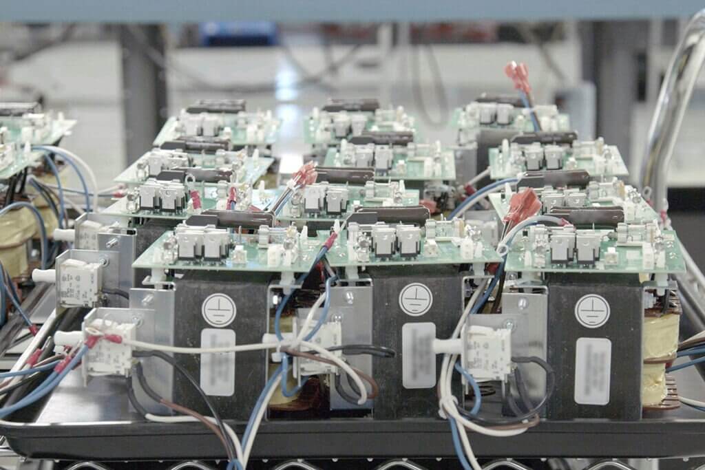
Aerospace and defense PCBAs use restricted-source semiconductors whose manufacturer date code and origin must remain associated with the program record. The risk is that mid-run lot substitutions can occur during part shortages, resulting in complete requalification instead of a straightforward restock. While X-ray inspection may uncover hidden solder defects, serialization and material records maintain the approved source and lot identification of the part; they cannot mitigate the risk of an undocumented substitution.
Medical Device PCBA
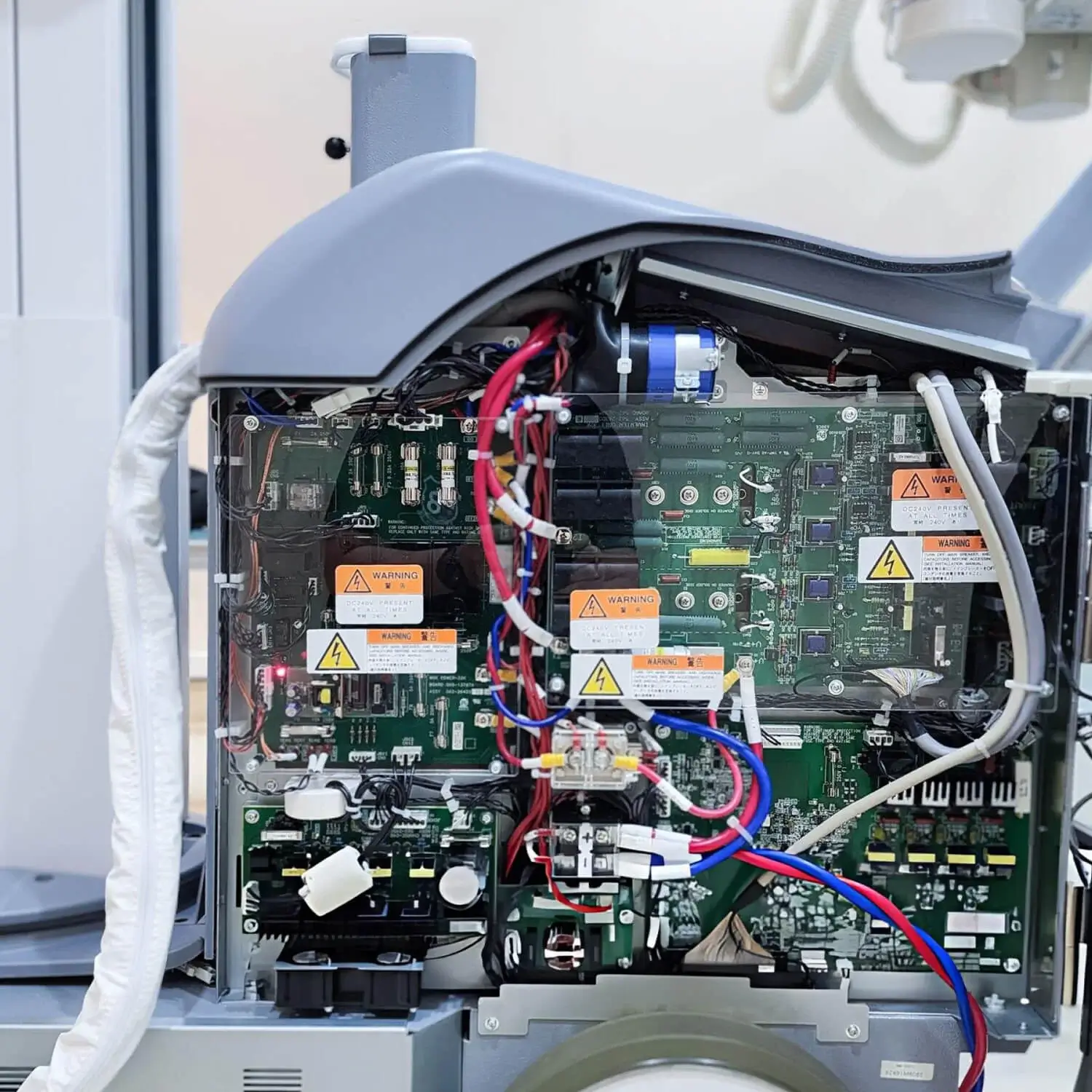
Medical diagnostic and wearable medical device assemblies use validated-lot sensors linked to the DHF. The risk is that a sensor lot swap may pass inspection and FCT, but the calibration baseline may shift enough to fail a downstream clinical check. This failure can only be traced to the source lot if the lot link is maintained through the kitting process.
Automotive Electronics PCBA
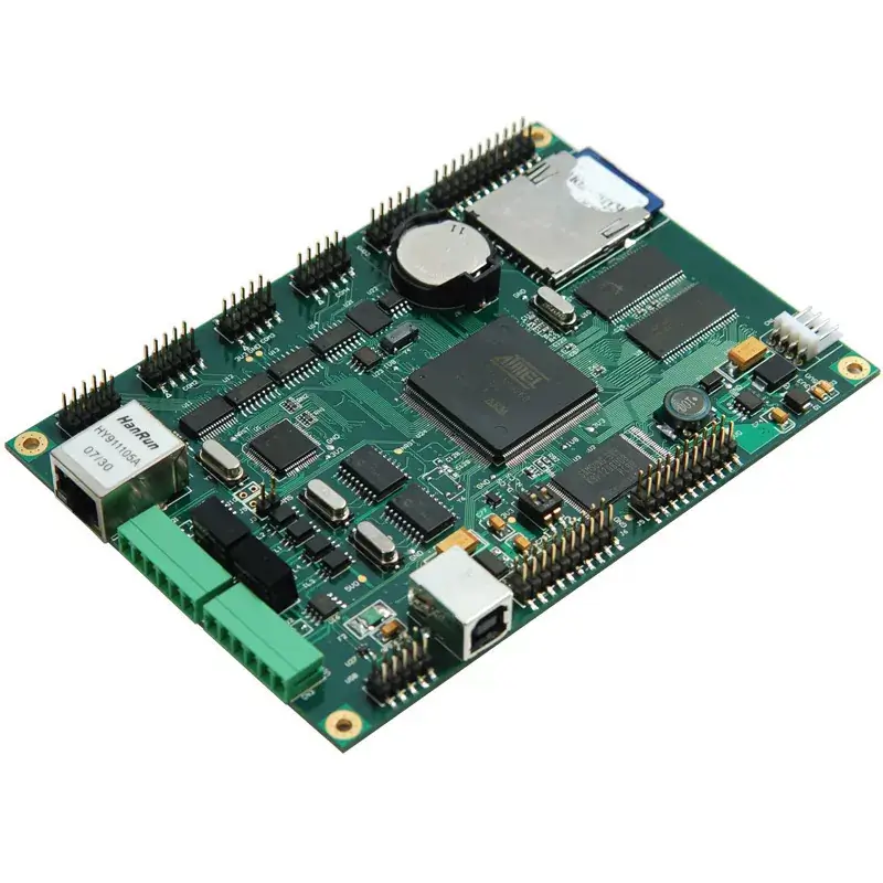
Automotive electronics use qualified microcontrollers and power devices from approved source lists across multiple plants. AOI and FCT can check for bad joints or open circuits. Neither will confirm whether the installed part came from the approved source and lot. The gap is that an unapproved-source lot may pass a board-level test but fail to perform correctly due to timing or EMC behavior when installed in a vehicle months later; this is the gap traceability aims to close.
Industrial Automation PCBA
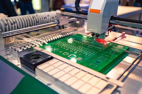
Industrial automation PCBAs use legacy automation boards and PLCs containing customer-held obsolete ICs alongside standard through-hole components. The concern is not reordering obsolete stock, which may have limited availability, but first-article timing. Running the full lot before confirming the solder profile and insertion settings can result in scrapped components that cannot be replaced through a new purchase order.

Communications Equipment PCBA
Communications equipment PCBAs depend on customer-approved transceivers and custom magnetics chosen for their ability to provide signal integrity over high-speed interfaces. A revision change might pass electrical open/short testing and ICT but fail under live traffic, since X-ray imaging confirms only the joint, not the signal margin. To identify a failed revision, live-traffic testing is required.
Energy Storage PCBA
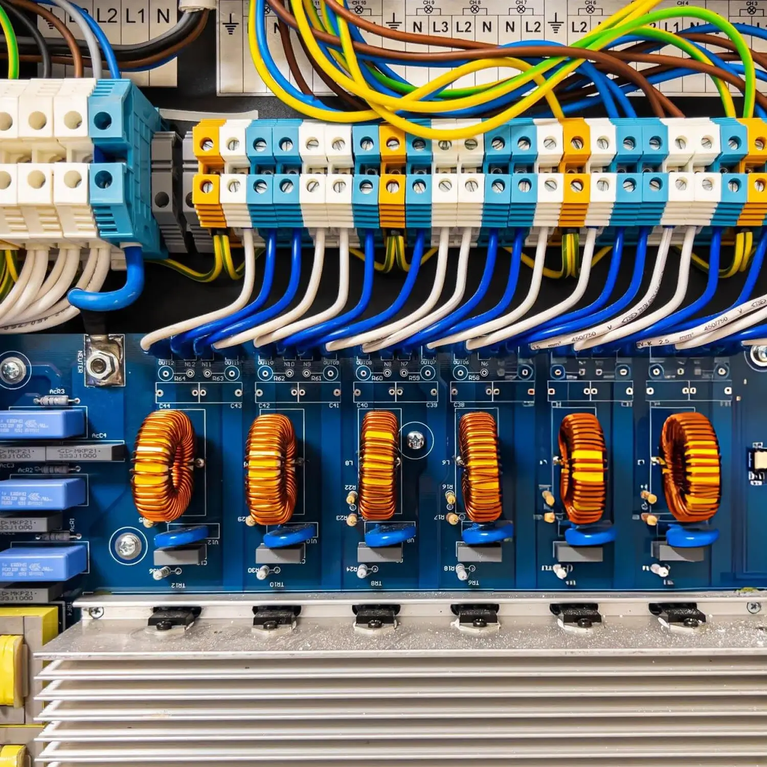
Energy storage PCBAs rely on customer-qualified isolation and current-sensing components specific to a single cell platform. A sensing-lot mismatch does not necessarily cause the board to fail, but it can shift the calibration of the protection thresholds. Therefore, testing must validate the installed lot against the actual limits of the cell platform rather than only verifying the physical footprint.
Consumer Electronics PCBA
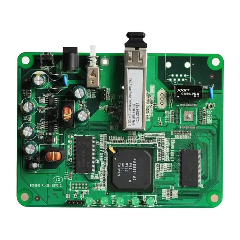
Consumer electronics PCBAs include wearable devices and compact products that use allocated processors for fast product-development cycles. The common issue is not the physical placement of miniature SMT components; rather, it is leftover inventory from a superseded revision being inadvertently added to a different production run without a clear carry-forward or scrap authorization.

LED Electronics PCBA
LED electronics PCBAs include lighting and display assemblies for which customers have selected specific LED binning groups to maintain color consistency and efficiency. An LED from one approved binning group mixed with an alternate bin may pass electrical testing but produce significant color variation across a shipment. Therefore, the LED bin identity must remain linked to material labels, kitting records, and placement records, while illumination testing confirms the result rather than the part number alone.
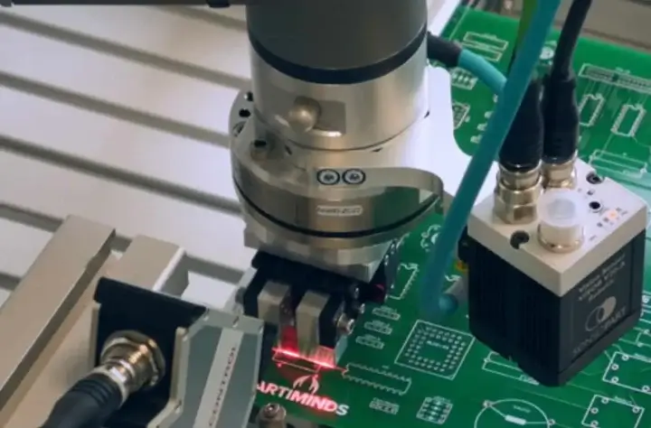
Robotic Control PCBA
Robotic control PCBAs use boards composed of customer-programmed processors and scarce motor-control devices. The risk is that the processor may contain the wrong firmware version. Although the board may pass assembly and electrical testing, incorrect firmware-hardware pairing can stall system commissioning because functional pairing between the encoder and I/O must be confirmed during firmware-hardware testing, not during solder-joint verification.
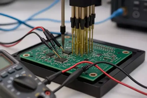
Test and Measurement Equipment PCBA
Test and measurement equipment PCBAs use customer-calibrated references and low-drift oscillators. The concern is maintaining the link between component serial numbers and calibration certificates through kitting. A test and measurement board may pass all electrical tests yet ship without an established calibration traceability chain.
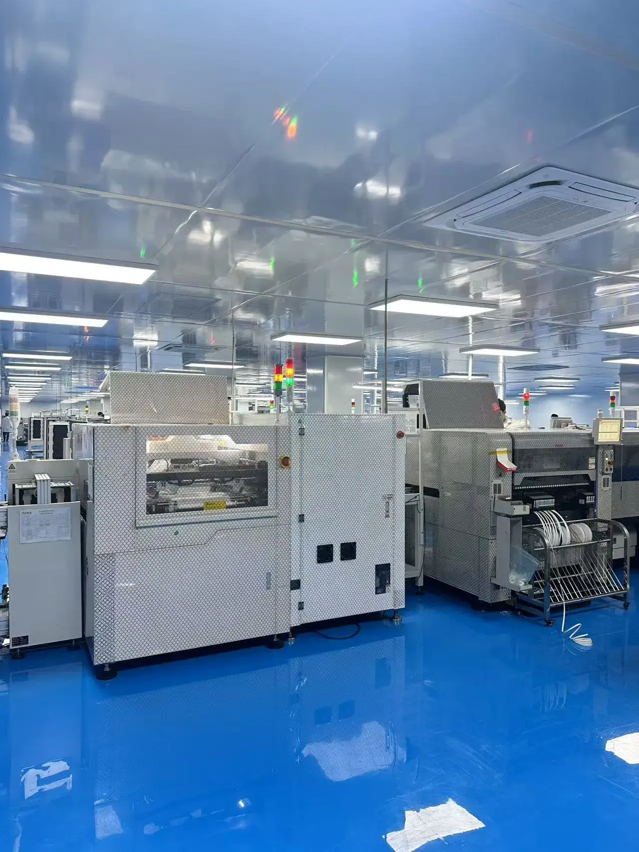
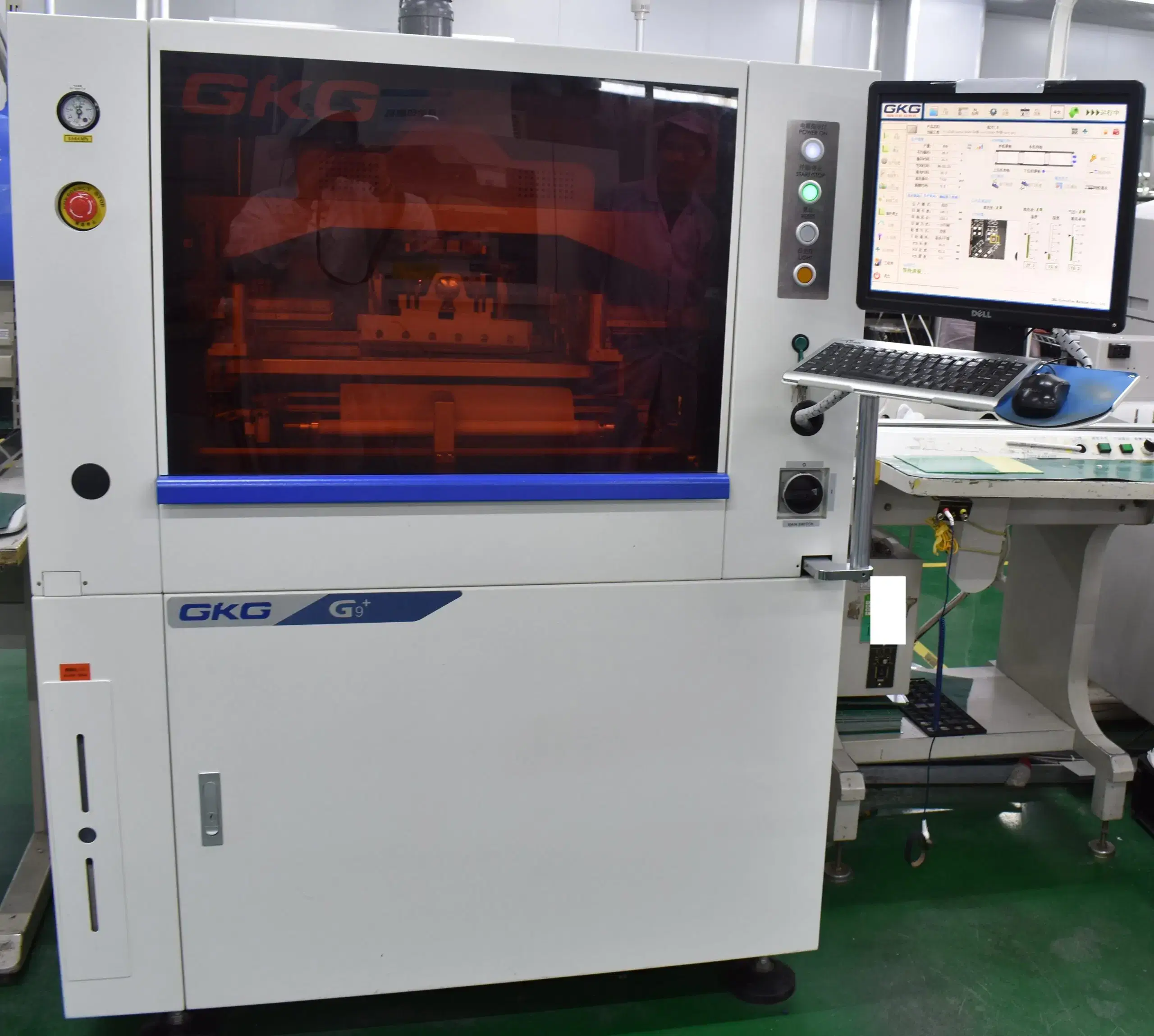
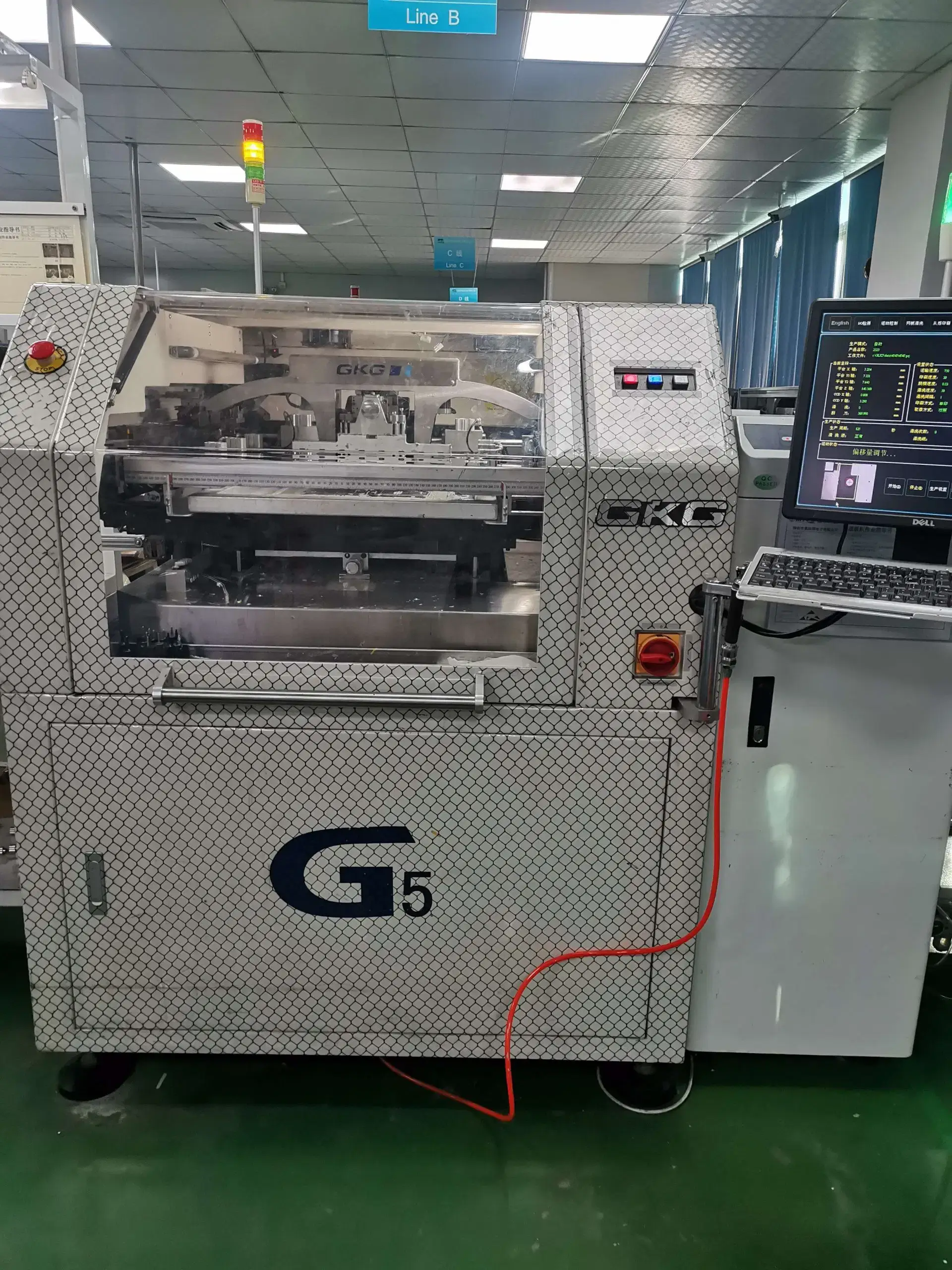
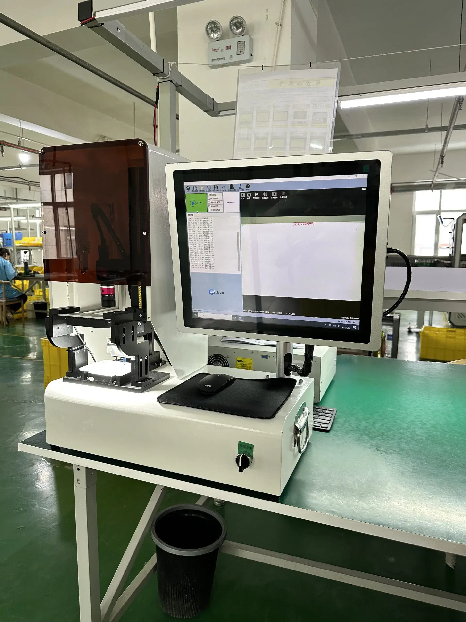
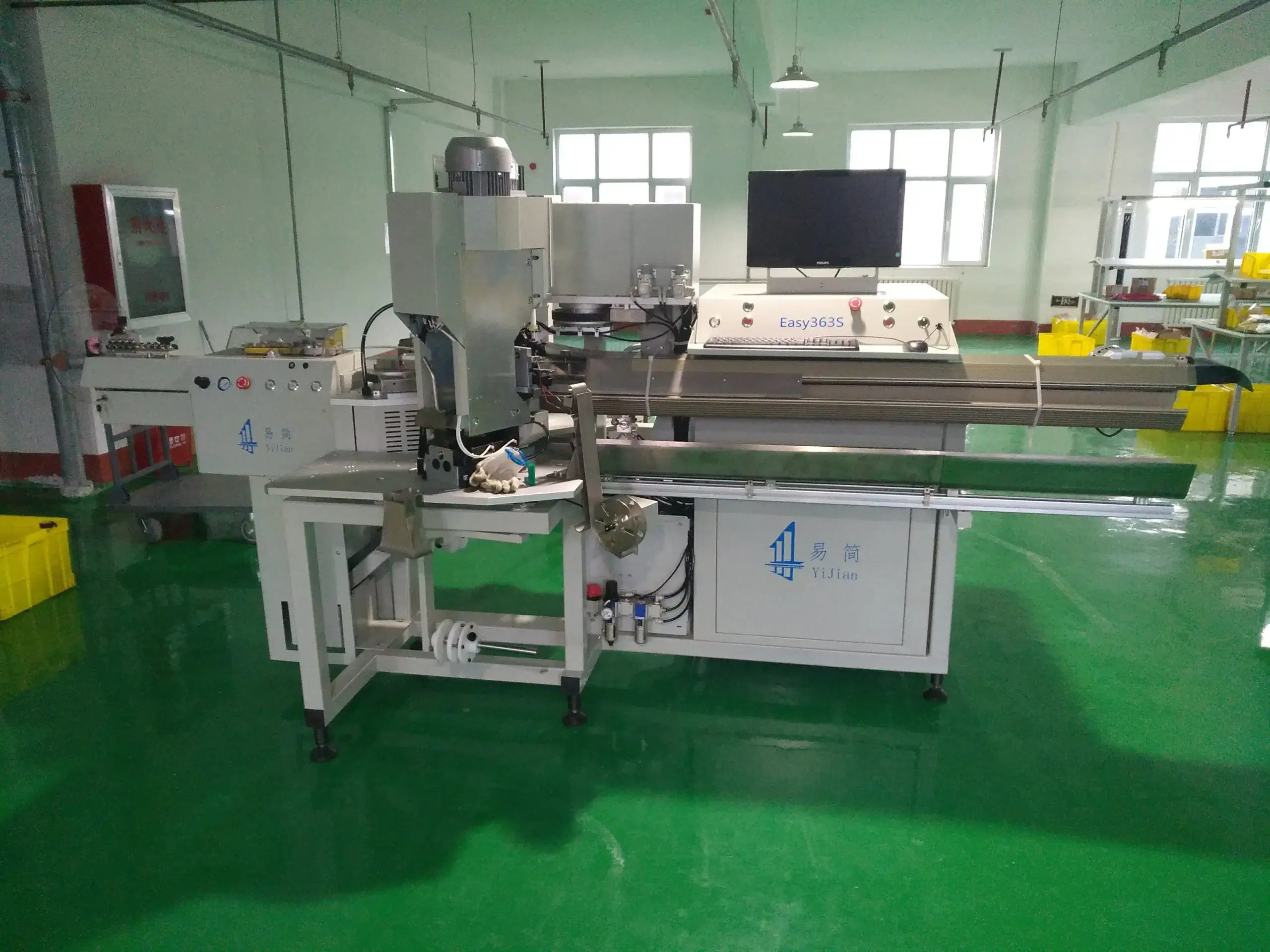
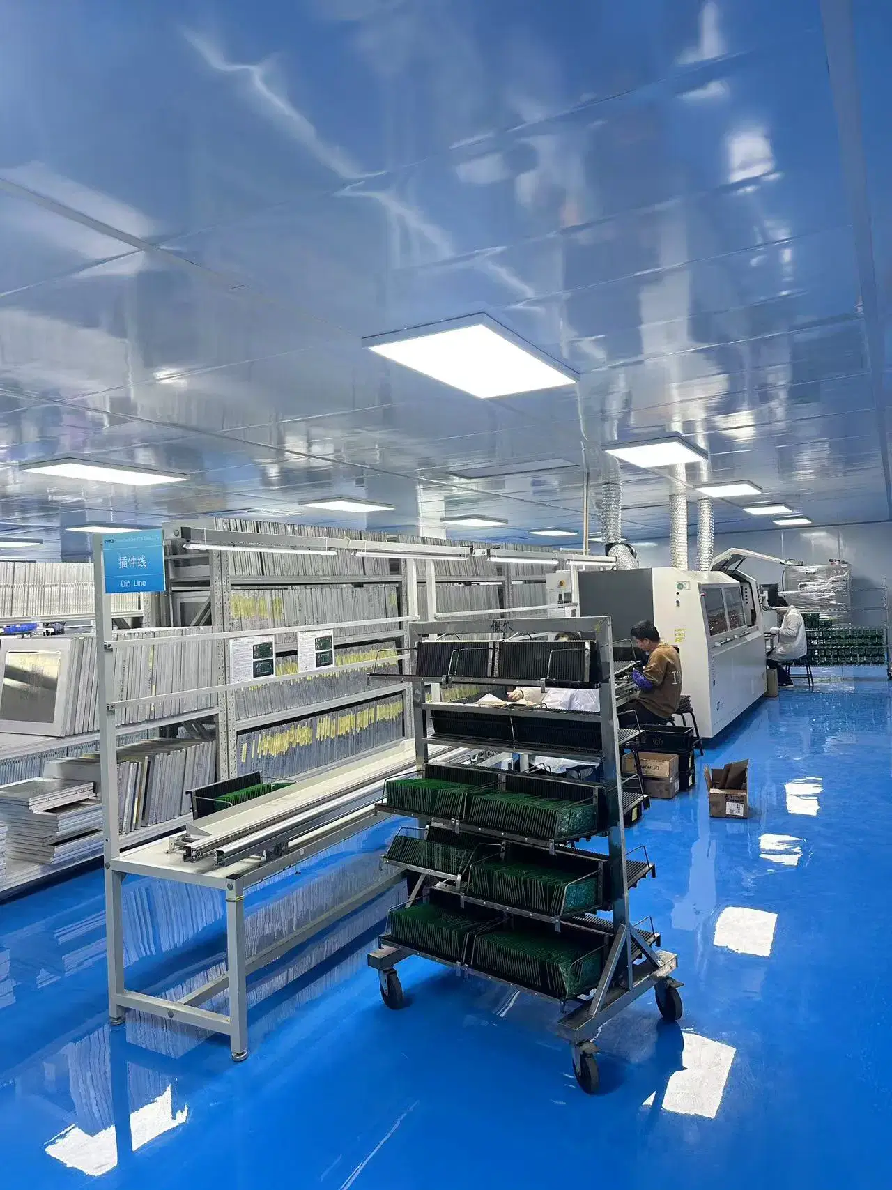
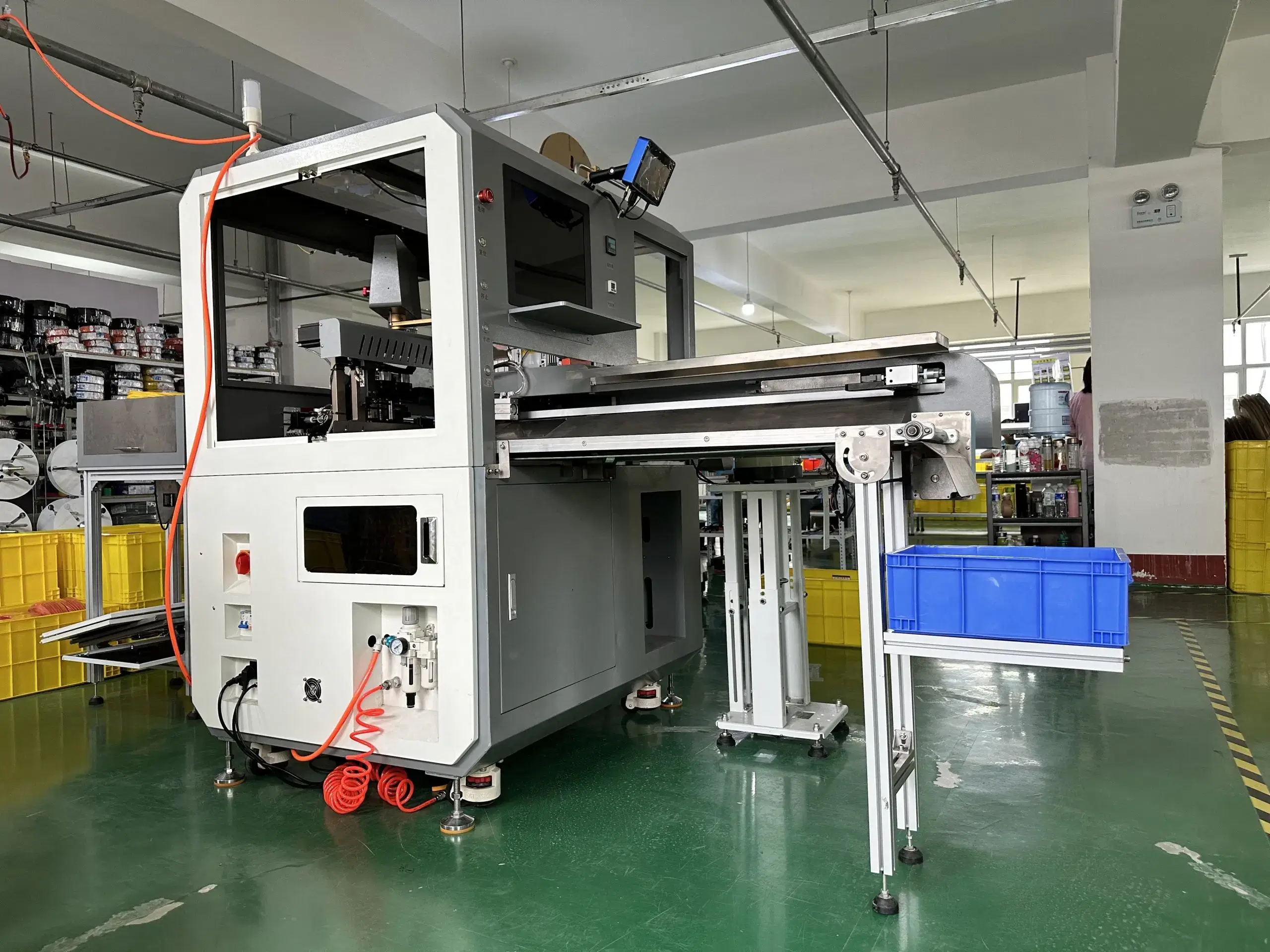
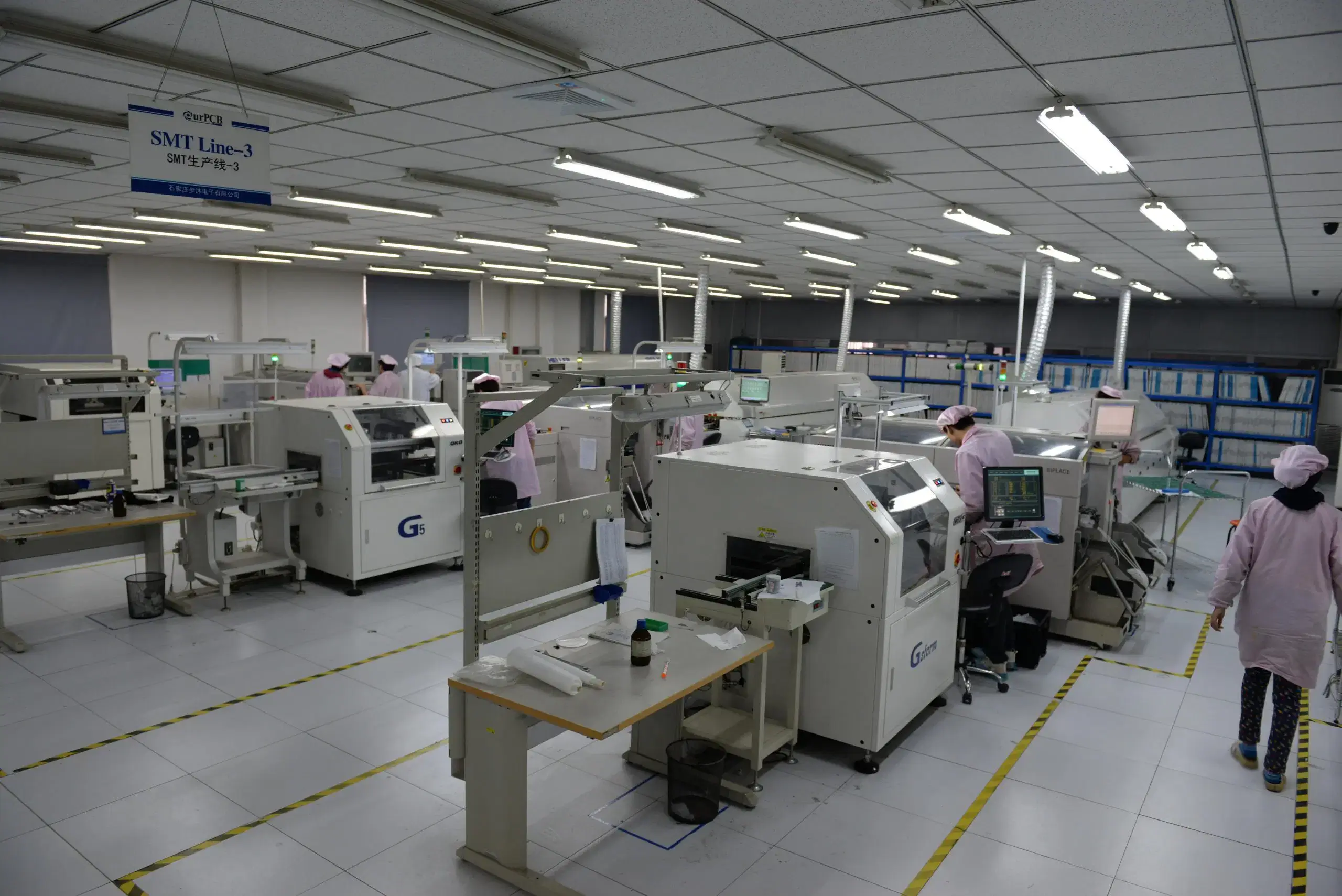
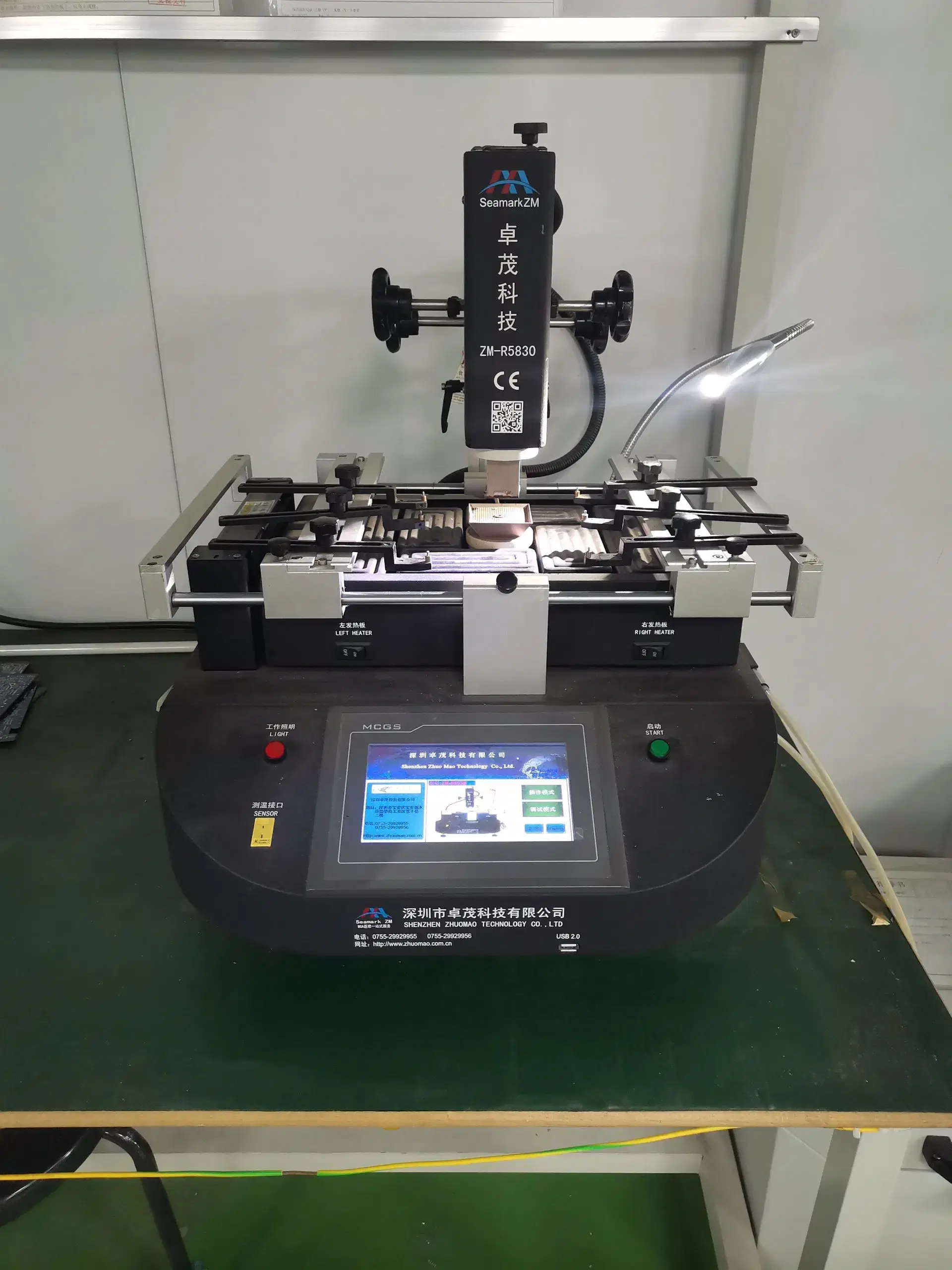
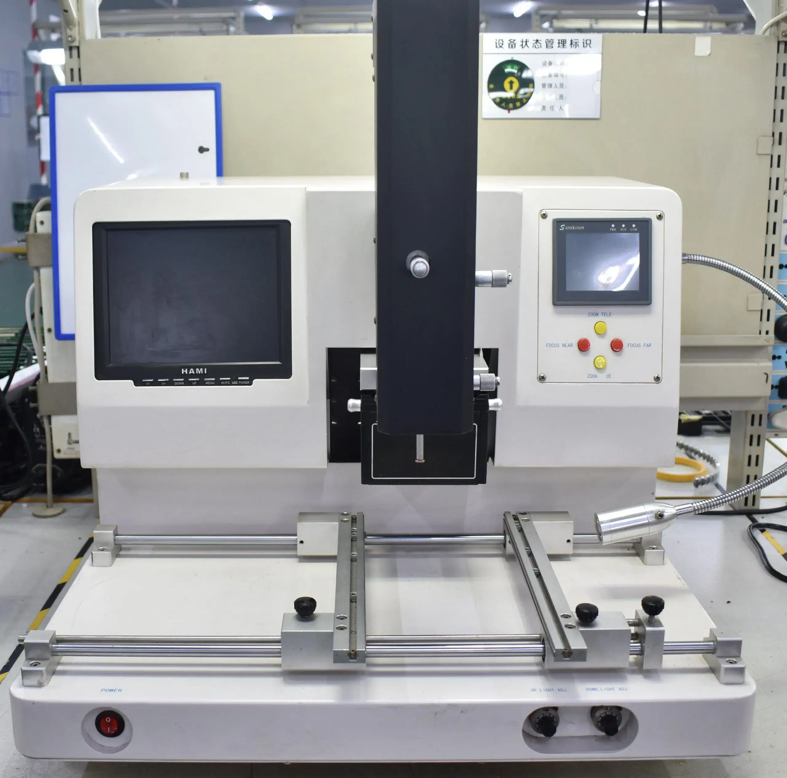
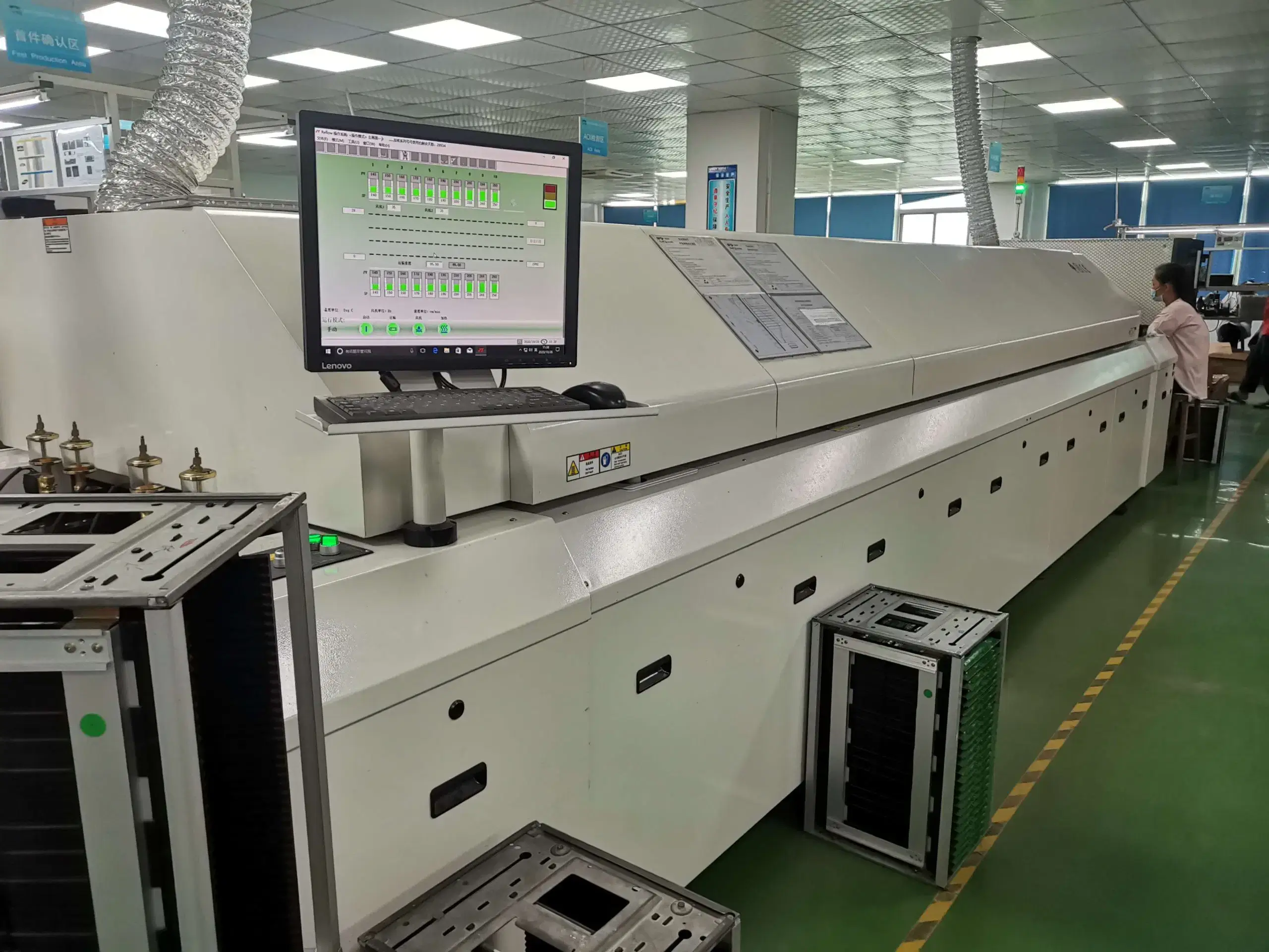
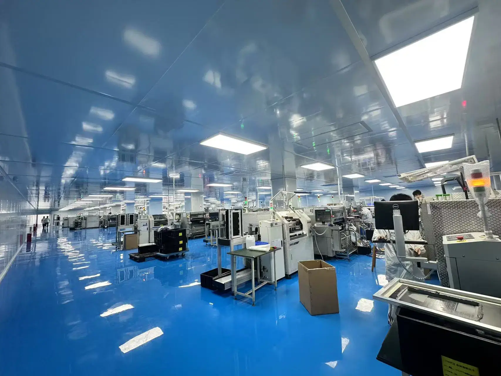
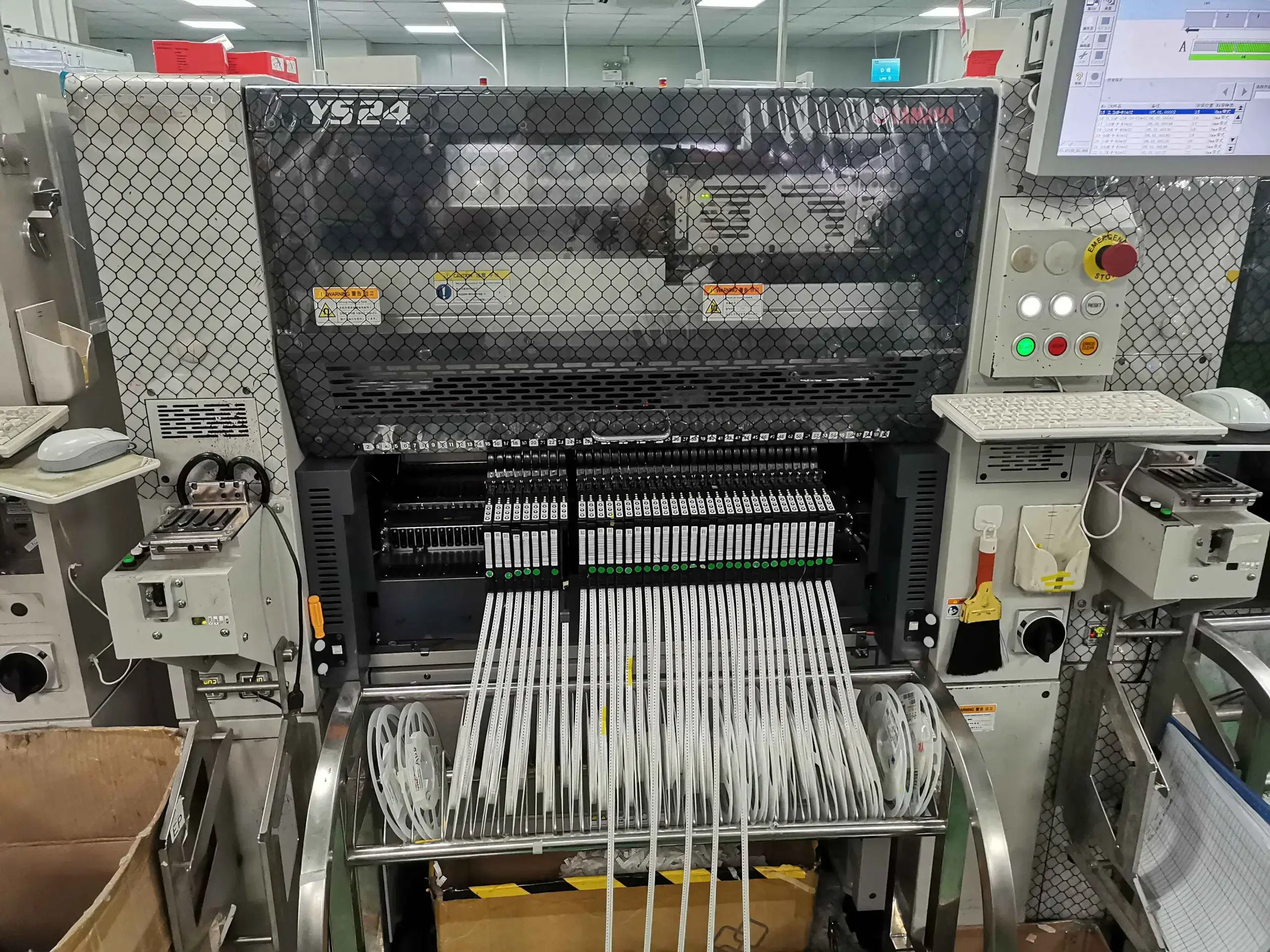
Our PCB Factory Gallery

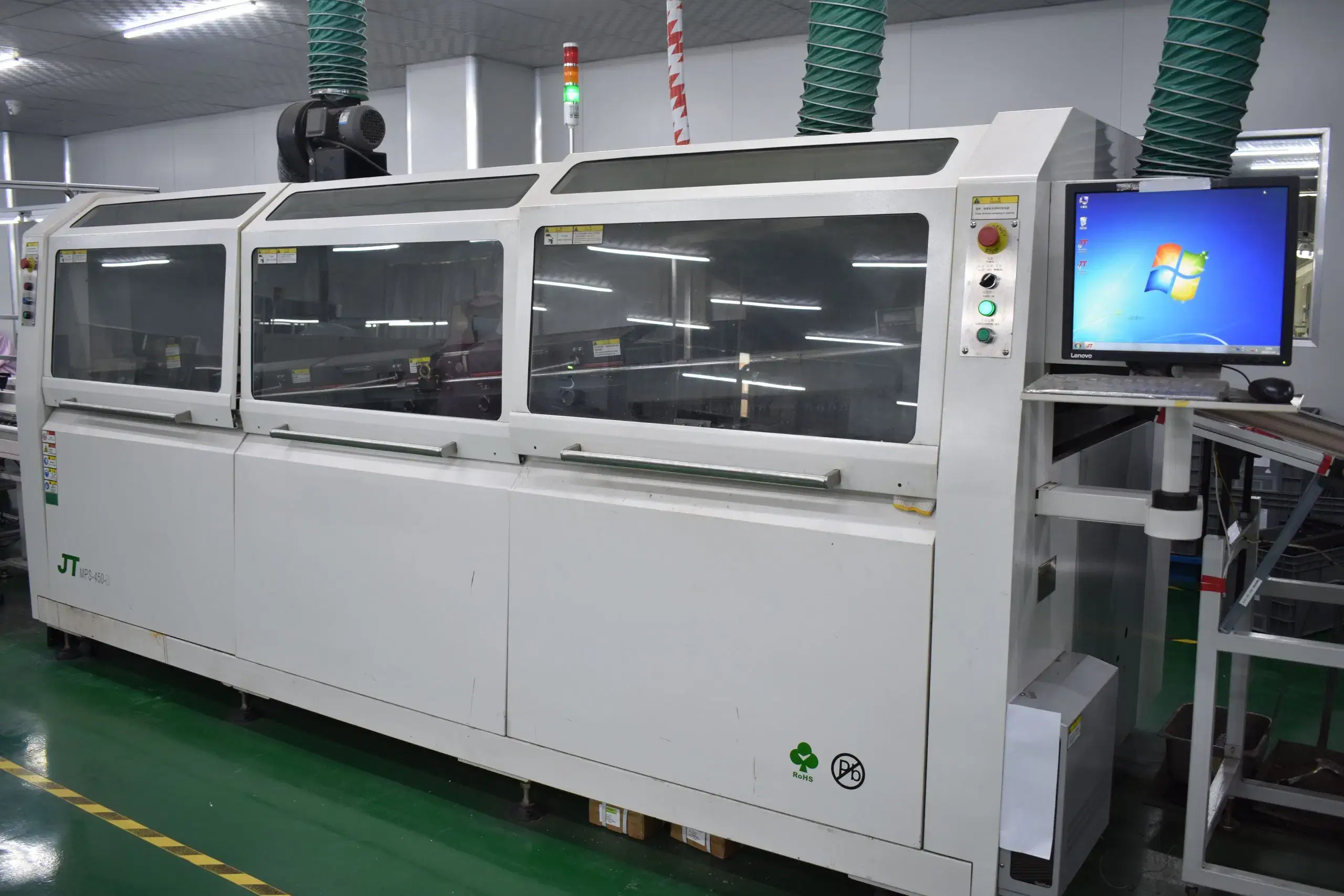
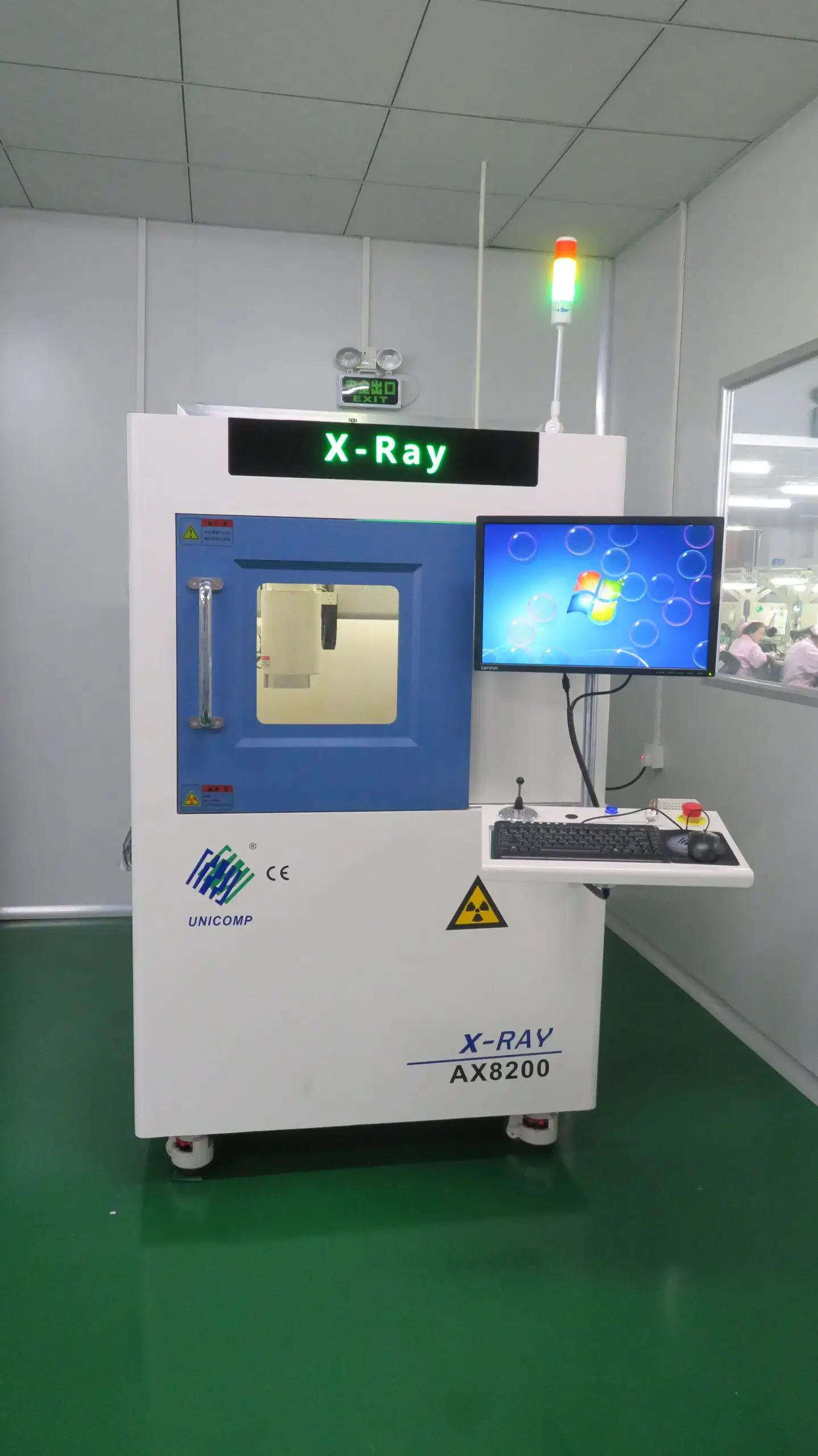
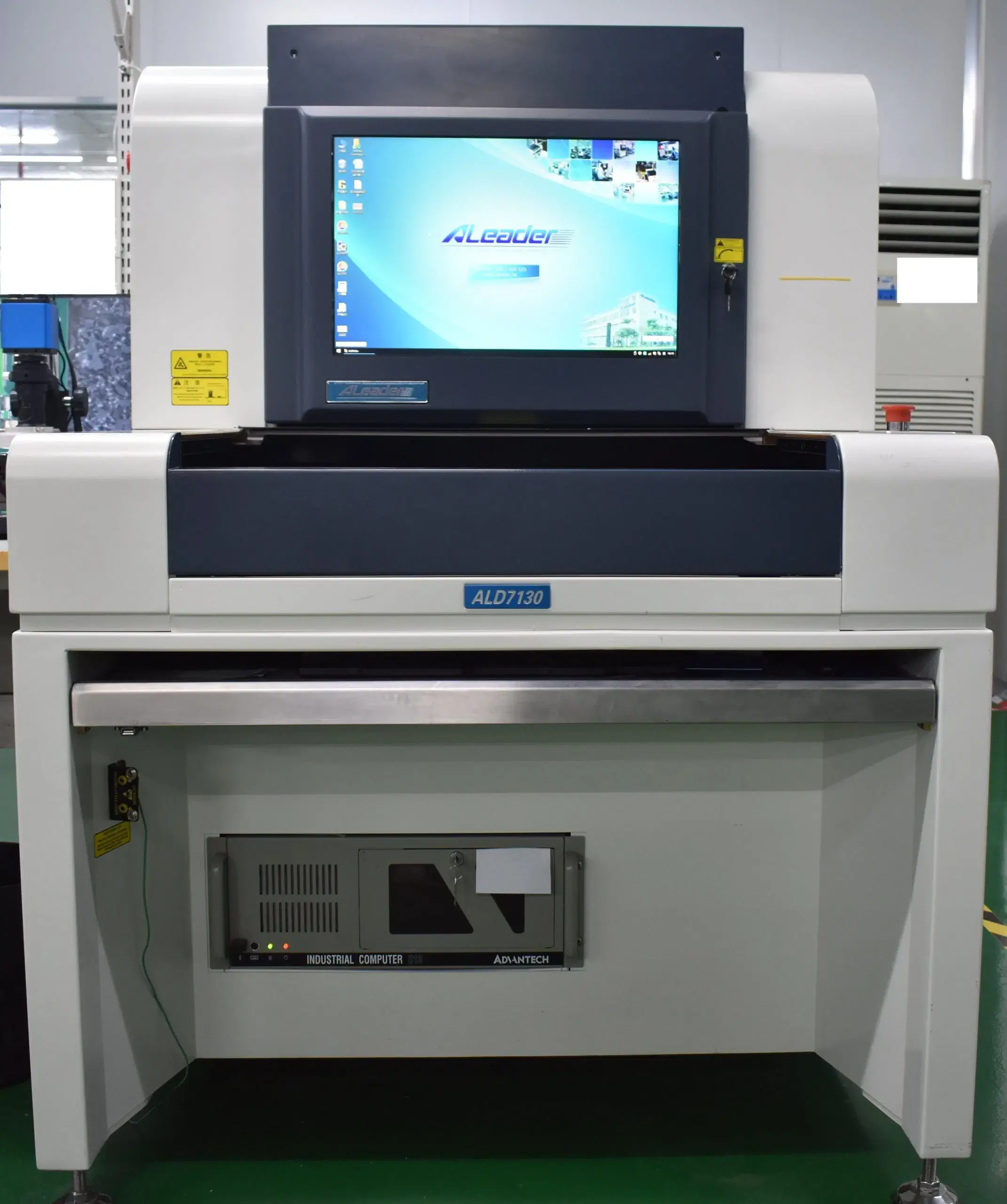
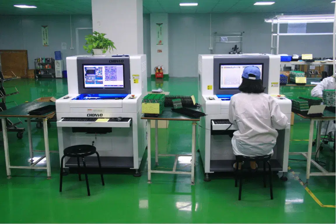
Frequently Asked Questions
PCB assembly costs depend on many factors, including the placement count, the proportion of SMT/THT, whether there are any fine-pitch or hidden-joint packages, the methods of handling the panels, whether the kits are complete, tooling and stencil costs, the extent of inspection and testing, expected rework costs, and the quantity ordered. Parts supplied by customers do reduce SUGA's sourcing responsibilities, but incoming verification, kitting, setup, soldering, inspection, testing, and material reconciliation will still incur costs.
A PCB is the bare board before component placement, while a PCBA is an assembled PCB that consists of components populated using SMT, THT, or mixed processes and has passed the inspections or tests performed during production.
Yes, SUGA uses partial reels or cut tape when the part identity and quantity can still be confirmed based on what is noted on the reels, trays, or tubes. A partial reel that has a short leader or an unlabeled tray will be either kitted manually or repackaged prior to being sent to the line for use, which adds additional kitting time that a complete reel would not incur. SUGA flags the exception when it receives the parts, not when it places them.
If the consigned parts are missing, mismatched, or fail inspection, SUGA will separate the affected BOM line and note the exact shortage, identity conflict, or defective condition of the part. Acceptable materials can continue to be tracked, but the affected step does not continue through a silent substitution. The affected item cannot be returned to production until there has been an approved supply or disposition decision.
Depending on which of the proposed actions—return, controlled storage, or carry-forward into the next approved lot—is selected, the customer will notify SUGA of the action to be taken once the material balance is complete. If the customer does not provide direction, SUGA will maintain the inventory in a controlled storage area, and the parts will be re-verified against the next revision before being issued to the kit.
Yes. A bare PCB can be supplied under full consignment as long as the board's identity, revision, quantity, packaging condition, surface condition, panel format, and assembly compatibility have all been validated through the incoming and engineering checks. The requirement to check the supplied PCB against the assembly data and component geometry remains.
A BOM revision can be controlled through revision-control procedures, but the BOM, placement data, drawings, ownership of the material, received quantities, feeder setup, machine program, stencil suitability, and test program must all be assessed together. All old-revision inventory and related records will remain separate until all affected items have undergone an approved use, return, rework, or replacement decision.
Lead times are determined by the stage of development the project is in; for example, whether it is a fully prepared prototype or a partial-kit production lot. The way lead time shifts is based mainly on whether the kit is complete. A complete, revision-closed kit will allow the project to remain at the fast end of its range. A kit with any missing BOM lines or unresolved revisions will affect the time to completion regardless of order size.