Upload BOM & Gerber
-
Mobile: +86 13312967631
-
Email: sales@sugaintl.com

Through Hole PCB Assembly Services
Durable Through Hole PCB Manufacturer in China For High-Stress Electronics
SUGA performs mechanical assembly of through-hole components and mixed THT and SMT components to form more complex assemblies. The assembly process includes all stages, from component preparation and insertion to lead control and soldering, followed by inspection, testing, and cleaning.
Up to 40 layers
Up to 1000 μm copper
8 wave soldering lines
4 selective soldering lines
What Is Through-Hole PCB Assembly?
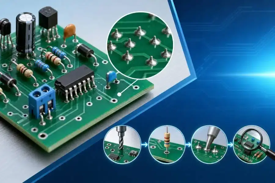
Through-hole assembly involves assembling components onto the PCB. A component lead placed in a plated component hole is connected to the PCB through a surface pad with an annular ring that forms the designed solder joint between the component lead and the PCB.
Through-Hole Components
Through-hole assemblies require components with leads of sufficient length to extend through the holes in the PCB. Axially configured parts, such as most resistors, have one lead positioned at each end of the body. Radially configured parts, such as capacitors, have both leads on the same side of the body. Other components, such as transformers and relays, are placed on the PCB using through holes when their mass, current, operating force, or other requirements justify additional mechanical support. Component lead geometry also affects the mechanical assembly work required.
When assembling through-hole component leads, the operator or insertion machine must maintain control of the identity, polarity, seating height, and body clearance of each component while allowing access to the solder side of the PCB. In many instances, THT is mixed with SMT, with SMT used for dense control electronics and THT used at mechanical or high-current node locations.
Plated Through Holes
A PTH offers a way to mount an electrical component on a PCB, providing both an electrical path to the component and a mechanical attachment to the PCB through soldering.
Through-hole PCB assembly can be implemented in many different kinds of PCB designs. IPC-2221C and other IPC design rules govern the relationships among a component lead, a through hole in the PCB, and a solder pad for electrical components. Therefore, the component drawing defines the final geometry when evaluating through-hole components to be assembled.
How Does a PTH Joint Hold Leads?
When the solder joint between the component lead and the plated barrel of the through-hole PCB is created, the PTH provides mechanical strength and electrical and thermal conductivity between the PCB and its component. Each part of the PTH solder joint is identified by its physical characteristics, such as wetting at the component lead, filling the plated through-hole barrel, and creating a fillet on the bottom surface of the PCB.
PTH solder joints should be clean on the bottom, while the barrel of the PTH requires evaluation to determine whether there is adequate solder fill.
When Should You Choose Through-Hole Assembly?
Through-hole assembly is ideal when an electrical component may experience repeated mechanical force, may carry substantial electrical current or mechanical load, may be repeatedly subjected to vibration or temperature changes, or must remain accessible for replacement. Use SMT assemblies when a lower-profile design, compact size, and higher density are desirable.
| Item | Design Impact | If Missing | Affected Result |
|---|---|---|---|
| Connector insertion or extraction load | The joint must resist repeated mechanical force | Surface pads may carry more peel stress without adequate support | Connector retention and field life |
| High current or high component mass | Larger leads and bodies need stable attachment and sufficient thermal design | Heat and weight can concentrate stress at the termination | Power delivery and thermal durability |
| Vibration, shock or thermal cycling | Joint geometry changes how repeated stress reaches the pad and barrel | Intermittent opens can appear after environmental exposure | Reliability in harsh service |
| Planned component replacement | Accessible leaded parts can support diagnosis and controlled replacement | Dense or inaccessible joints increase repair damage risk | Prototype iteration and serviceability |
Which Parts Need Mechanical Retention?
Mechanical retention is necessary whenever a daughterboard or cable moves and generates mechanical loads in the PCB through the connectors inserted into the PCB. Similarly, the mechanical loads imposed by switches, terminal connectors, and power connectors with soldered leads can affect PCB connections when a part is moved. Switches, terminals, and sockets also impose loads on PCB connection points. When larger magnetic components are incorporated into a PCB, their added mass creates additional mechanical loads during movement or vibration.
Brackets, adhesives, fasteners, enclosure mounts, and other supporting components act as load paths for connectors before mechanical loads reach the connectors and the pads they connect to.
High-Power Components
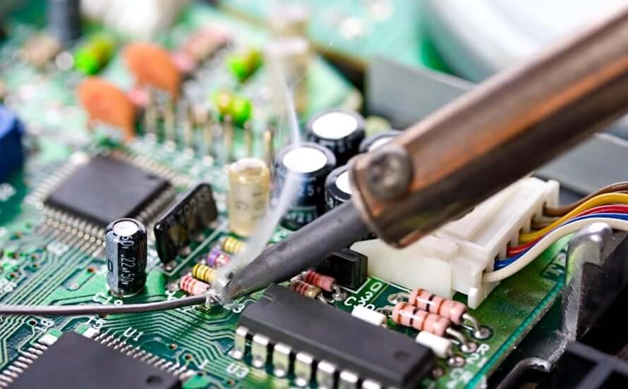
Transformers, large capacitors, power connectors, relays, and selected power devices often have large leads and substantial component mass combined with high current and heat generation. For instance, large through-hole terminations can create stable attachment points and conductive paths. Space and clearance around transformer housings also allow for insulation and heat management. Copper thickness, conductor width, creepage distance between conductors, clearance between the PCB and the part, thermal interfaces, and heat sinks for transformer housings should also be defined early in the design and manufacturing process.
Harsh-Environment Nodes
Though the mechanical retention methods described above may not correct issues with vibration and thermal cycling, they will change how much of those loads is transmitted to the connection joint. The mechanical retention of a connector will have different characteristics from the mechanical retention of a transformer subjected to constant vibration. Therefore, the mechanical retention method should follow the unique load path rather than a generic “harsh environment” classification.
While THT mechanical retention methods are still useful when thermal-cycling and vibration test records for similar PCB designs exist, additional mechanical retention methods should also be employed at the same connectors where THT retention is used. However, while THT retention applied to the connector lead and barrel reduces movement at the junction where the lead meets the PCB, different materials have different thermal expansion properties, so material expansion continues to create additional loads on the connector.
Prototype Rework
An accessible leaded part improves the technician’s ability to diagnose, repair, or replace the part during prototype development. Sockets and leaded components provide an additional advantage by allowing technicians to reach the leads and remove the part without damaging the package.
Heat and extraction force must also be controlled. Excessive temperature or mechanical loads can damage a solder pad or plated barrel, while thick copper can draw heat away from the solder joint. IPC-7711/21D documents rework, modification, and repair methods for PCB designs and component types.
SMT vs. Through-Hole Assembly
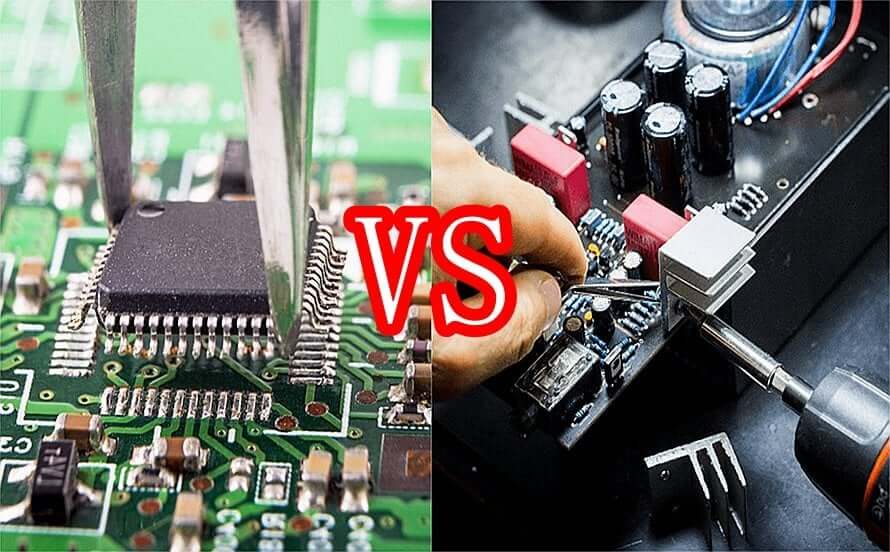
SMT is ideal for assembling densely populated PCB layouts with very small surface-mount parts and double-sided PCBs, while THT supports through-hole connections for larger parts, heavier loads, and mechanically stressed connections.
| Comparison Factor | SMT | Through-Hole | Assembly Impact |
|---|---|---|---|
| Termination geometry and load path | Components terminate on surface pads | Leads pass through plated holes and are soldered to the barrel and pads | Choose by package termination and the force transferred into the PCB |
| Component density and package range | Supports small parts and fine-pitch packages in compatible processes | Leaded bodies and hole spacing normally use more board area | Dense control sections favor SMT; leaded power and electromechanical zones may favor THT |
| Double-sided placement and keep-outs | Well suited to dense placement on both sides | Lead protrusion, body height and solder access can restrict the opposite side | Reserve component and soldering keep-outs before fixing the mixed-board layout |
| Mechanical and environmental loading | Reliability depends on package, pad, support and service conditions | Lead-and-barrel retention can better support mating force, mass and selected vibration loads | Match the retention method to the specific load path: a connector under repeated mating force needs different support than a transformer under constant vibration |
| Power and thermal requirements | Compact power packages can work with compatible copper and thermal design | Large leads and bodies suit many transformers, relays, capacitors and power connectors | Select by current, heat, clearance, copper mass and component availability together |
| Automation, throughput and total cost | Placement is highly automated and supports high component counts | Insertion, wave, selective or manual operations can add handling and process-specific setup | Sum insertion, soldering, masking, inspection and rework across the whole board, since SMT and THT carry different cost profiles per operation |
| Rework and serviceability | Dense or fine-pitch packages may require specialized rework equipment | Accessible leads can simplify controlled replacement | Accessibility, heat demand and pad/barrel protection determine practical repairability |
| Component compatibility | Broad for modern compact ICs and passives | Strong for leaded power, connector and electromechanical packages | Mixed assembly preserves the best available package for each board function |
| Reliability and lifecycle consequence | Can be highly reliable when design and process match the environment | Can provide robust retention where mechanical load dominates | Lifecycle reliability depends on design, process control, support structure and validation |
Board Density
In multilayer PCBs, component holes reserve space on every layer they pass through, not only on the top side. Once the layout is fixed, it becomes very costly to reverse decisions about board density. When making decisions on board density, the practical design-review question is not “is it an SMT part or a through-hole part,” but rather “what specific nets can tolerate the keep-out area associated with a plated hole without increasing the size of the board outline?” The design team should identify each connector, power component, and relay at the outset of the design cycle and confirm that its footprint and clearance are appropriate for the rest of the layout before committing to the board outline, because moving a THT part at the end of the design cycle will cost substantially more in rerouting than moving an SMT part.
Zone the layout early. One application is to mount dense logic components using SMT while using THT for a transformer, relay, or connector where its package and load require it. The benefit of zoning in this instance is that you do not have to create a low-density mounting style for all components on a PCB or squeeze leaded parts into areas that are unsuitable for soldering.
THT Cost Drivers
Using automatic insertion for compatible axial and radial leaded components, the touch time required to assemble these components is reduced. The cost of setting up the automatic machine and creating the program will be recovered once the volume justifies the setup cost, after which the exposed leads can be soldered in one continuous operation using a wave soldering machine. The cost associated with selective soldering and manual insertion is calculated differently from automatic insertion because it is based on the time required to program the local joints and the manual touch time required to insert the components. When very few accessible leaded components are used in prototype work, the setup time will not be very large; however, as the number of leaded components and selective-soldering joints increases, the cycle time for the finished PCB assembly will also increase.
When Is Mixed Assembly Better?
Mixed assembly is best suited for situations where compact control electronics and larger, heavier connectors, transformers, relays, capacitors, or other leaded components carry load, power, or replacement duties on the same board. The layout will also need to include enough space for insertion, lead protrusion, nozzle access, or wave pallets before the layout is finalized, as most production operations place and reflow the SMT components first, then place and solder the through-hole components because this sequence reduces physical interference and avoids exposing the leaded components to unnecessary heat.
From Insertion to Final Test
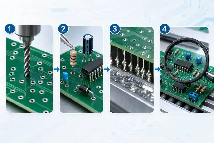
The process of through-hole PCB assembly includes five operations: component insertion, flux and preheat, soldering, post-solder lead control and cleaning, and finally inspection and test.
Component Insertion
Component insertion is often the final opportunity to correct component errors without exposing the assembly to heat. The operator or machine controls the part number, orientation, polarity, seating height, and body clearance of the component being inserted. Temporary retention or clinching can keep the leaded component in place after insertion; however, it must not obstruct solder flow or a selective nozzle.
Automatic insertion systems can handle axial and radial geometries at high volume. Manual insertion of connectors, terminals, transformers, or other non-standard components should be based on component form, lead condition, board accessibility, and assembly repeatability. Insertion is complete when each leaded part is stable and correctly positioned, with solder access preserved.
Flux And Preheat
Flux prepares the joint surfaces for soldering by removing oxides and aiding solder wetting of the lead, barrel, and pad. Preheating the PCB before soldering activates this chemistry and decreases the risk of thermal shock to the components being soldered. The process needs to heat light areas and high-thermal-mass regions in a controlled manner. Heavy copper, ground planes, and large leads will draw heat away from the joint.
The chemistry used should correspond with the product requirements, cleaning method, PCB finish, and solder alloy. With insufficient activation, wetting is poor. Excessive heat can damage materials or exhaust the flux too early. IPC-7530B guides temperature profiling for THT components based on PCB materials and thermal mass.
Post-Solder Finishing
Lead condition after soldering depends on the component and process and may require a post-solder trim to achieve the specified protrusion or clearance. The cutting process should not shock the joint, lift the pad, or damage the barrel.
Residue control should also match the product requirement and flux chemistry. For no-clean flux, the residue condition is assessed against cleanliness and electrical-clearance requirements. Checks include sharp ends, cleanliness, electrical clearance, and residue condition before inspection and test.
Through-Hole Soldering Methods
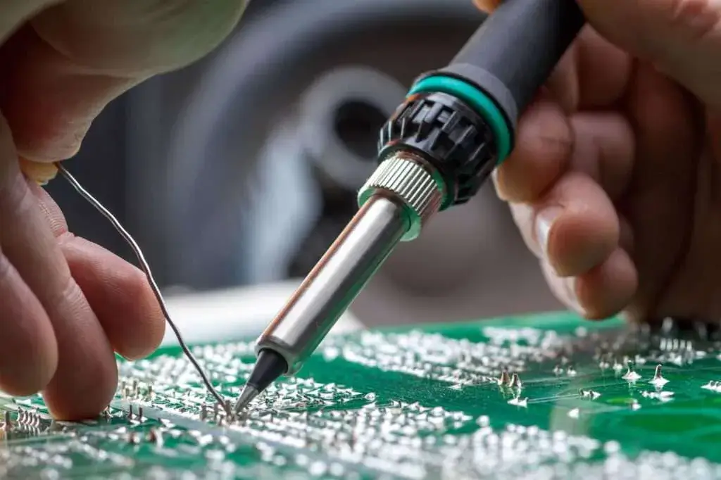
Wave soldering should be used when many accessible through-hole joints can pass through broad bottom-side solder exposure. Selective soldering is mainly used for mixed PCBs to assemble THT connections near SMT features. Controlled hand soldering can be used for prototypes, repair, low-volume work, and connections that cannot be reached with standard soldering machines.
When Is Wave Soldering Appropriate?
Wave soldering works best with stable designs that have many through-hole connections exposed on the solder side. The board travels over the heated solder wave on a conveyor, allowing each board to be soldered in one controlled pass. Even flux coverage, preheating, conveyor stability, solder contact, and board exit conditions all affect successful soldering. Component clearance and orientation affect solder drainage and shadowing.
Masks and pallets can protect non-target areas while providing access to the intended solder connections. If bottom-side SMT components fall outside the wave-soldering process window, localized selective soldering should be used.
Where Does Selective Soldering Protect SMT?
Selective soldering confines flux, heat, and solder contact to specific THT regions. When nearby SMT parts, pads, or geometries should not cross a full wave, selective soldering is preferred. There must be a workable nozzle path and a keep-out area around the solder flow. These requirements must be considered during layout rather than after the board is produced.
The distribution of solder joints affects cycle time. Variables include the fluxing location, nozzle size and shape, nozzle-path dimensions, local thermal mass, dwell-time consistency, solder height, travel distance, machine programming, and physical access limitations.
Hand Soldering For Complex Geometry
To maintain soldering quality, the operator controls variables such as tip condition, access angle, applied heat, dwell time, solder volume, work instructions, and solder-joint acceptance criteria. Because hand soldering is manual, throughput is lower than with wave or selective soldering; therefore, it is used for geometry exceptions while maintaining consistent workmanship.
How Are Through-Hole Defects Controlled?
To effectively control through-hole defects, the soldering operation must be performed with consistent flux, preheat, soldering conditions, and defined workmanship limits.
| Defect | Likely Cause | Detection | Prevention | Acceptance Result |
|---|---|---|---|---|
| Insufficient barrel fill | Inadequate heat, weak wetting, blocked access or poor lead-to-hole fit | Visual examination from accessible sides; X-ray or section analysis when internal condition must be proven | Balance preheat and solder contact; maintain solderable surfaces and workable clearance | Wetting and fill meet the specified workmanship class |
| Voids or incomplete internal wetting | Gas entrapment, contamination or unstable thermal conditions | X-ray or section analysis when risk justifies internal evidence; electrical checks for resulting opens | Control cleanliness, flux activity, material condition and thermal profile | Internal evidence and electrical result match the product risk and defined workmanship limits |
| Bridging | Excess solder, close spacing, poor drainage or unstable withdrawal | Visual inspection, AOI where geometry is visible, and electrical short testing | Manage lead length, orientation, solder contact and board exit conditions | No unintended electrical connection between adjacent conductors |
| Solder balls | Spatter, moisture, excessive flux activity or disturbed solder release | Visual inspection and AOI on visible surfaces | Control material condition, preheat, flux quantity and solder dynamics | No conductive debris that threatens spacing, insulation or reliability |
| Lifted pad | Excessive heat, mechanical force or repeated rework | Visual inspection and continuity checks around the affected connection | Limit heat and extraction force; use controlled rework technique | Pad adhesion remains acceptable and the electrical connection remains continuous |
| Damaged barrel | Drilling or plating weakness, excessive insertion force, thermal stress or aggressive removal | Continuity testing plus X-ray or section analysis when structural evidence is required | Protect hole plating during PCB fabrication, insertion, soldering and rework | Continuous electrical path with no unacceptable barrel separation or layer-connection damage |
How Are Solder Joints Inspected?
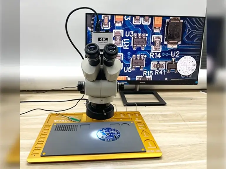
Accessibility to through-hole solder joints allows 100% visual inspection. Accessible areas can be assessed through visual inspection, including visible features such as polarity, bridging, and surface defects via AOI. Internal solder-joint inspection in selected areas utilizes X-ray technology.
ICT checks electronic components for defined conditions such as shorts, opens, and component-level electrical conditions. FCT verifies and characterizes the overall behavior of the circuit board under specified electrical loads and inputs. Mechanical inspection of solder joints provides evidence of their mechanical integrity, while the defined electrical nodes indicate the extent to which ICT and FCT verify the electrical integrity of those connections.
Incomplete Barrel Filling
Solder barrel fill is most critical for high-current, heavy-copper, or Class 3 applications. An under-filled solder joint may pass a simple visual inspection because the internal fill and heat transfer during soldering cannot be seen. Internal fill can be evaluated through X-ray inspection on a statistical basis, whereas the solder-fill level of an individual sample can be confirmed through destructive section analysis at the expense of the sample. Thus, the solder-fill status of heavy-copper or high-reliability builds remains unverified unless confirmed through one of these inspection methods.
Unwanted Solder Deposits
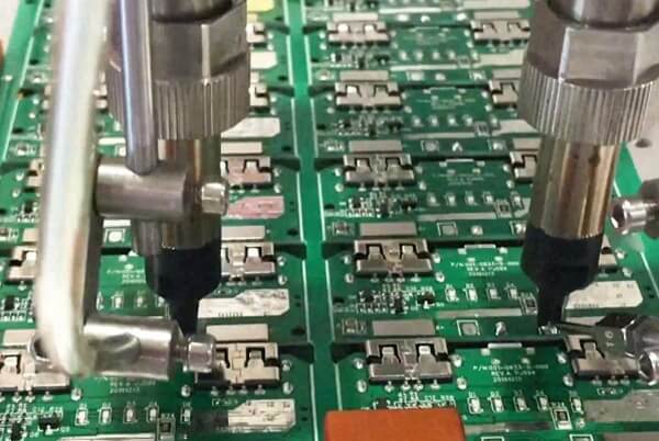
A bridging condition is detected immediately as an electrical short through AOI or electrical testing before shipment; however, a loose solder ball may remain undetected until vibration or handling causes it to move, possibly resulting in a bridge between conductors months later when the assembly is placed in service. Applications subject to vibration or housed in sealed enclosures require a cleanliness process that identifies loose solder balls, not only bridging, because loose solder balls and bridges may be detected at different inspection stages.
Copper Damage During Rework
When copper damage occurs during rework of a PCB, it is important to determine when the damage occurred, such as during fabrication, first-pass assembly, or a rework cycle, so that responsibility for repairing the PCB can be determined. Determining when the damage occurred provides a clearer understanding of whether the cause was drilling or plating defects or damage caused by component insertion or rework. Both types of damage can appear similar during visual inspection, but continuity testing combined with physical analysis can determine the cause with greater confidence.
For builds that have been subjected to additional rework cycles, it is advisable to ask the assembler to document the number of times the board or individual component locations have been subjected to rework. If no one tracks that information, the increased risk associated with additional rework is unlikely to be visible during a single inspection.
Acceptance Standards
IPC J-STD-001J defines requirements for soldering materials, soldering methods, process control, and verification. The acceptance criteria for finished assemblies are defined by IPC-A-610J. Rework, modification, and repair methods are defined in IPC-7711/21D, while temperature profiling for mass soldering processes is defined by IPC-7530B. Each standard addresses a different production-related issue.
SUGA executes IPC-A-610J Class 2 and Class 3 assembly in accordance with IPC workmanship standards, which define finished-assembly acceptance. However, the criteria for bare-board hole plating are part of the PCB fabrication process.
Through-Hole Assembly Applications
Through-hole assembly and mixed assembly are typically used where boards must support power components, connectors, mechanical loads, environmental stresses, or serviceable parts. Package type, solder accessibility, operating conditions, and testing requirements determine which components use THT connections.
Power Supplies
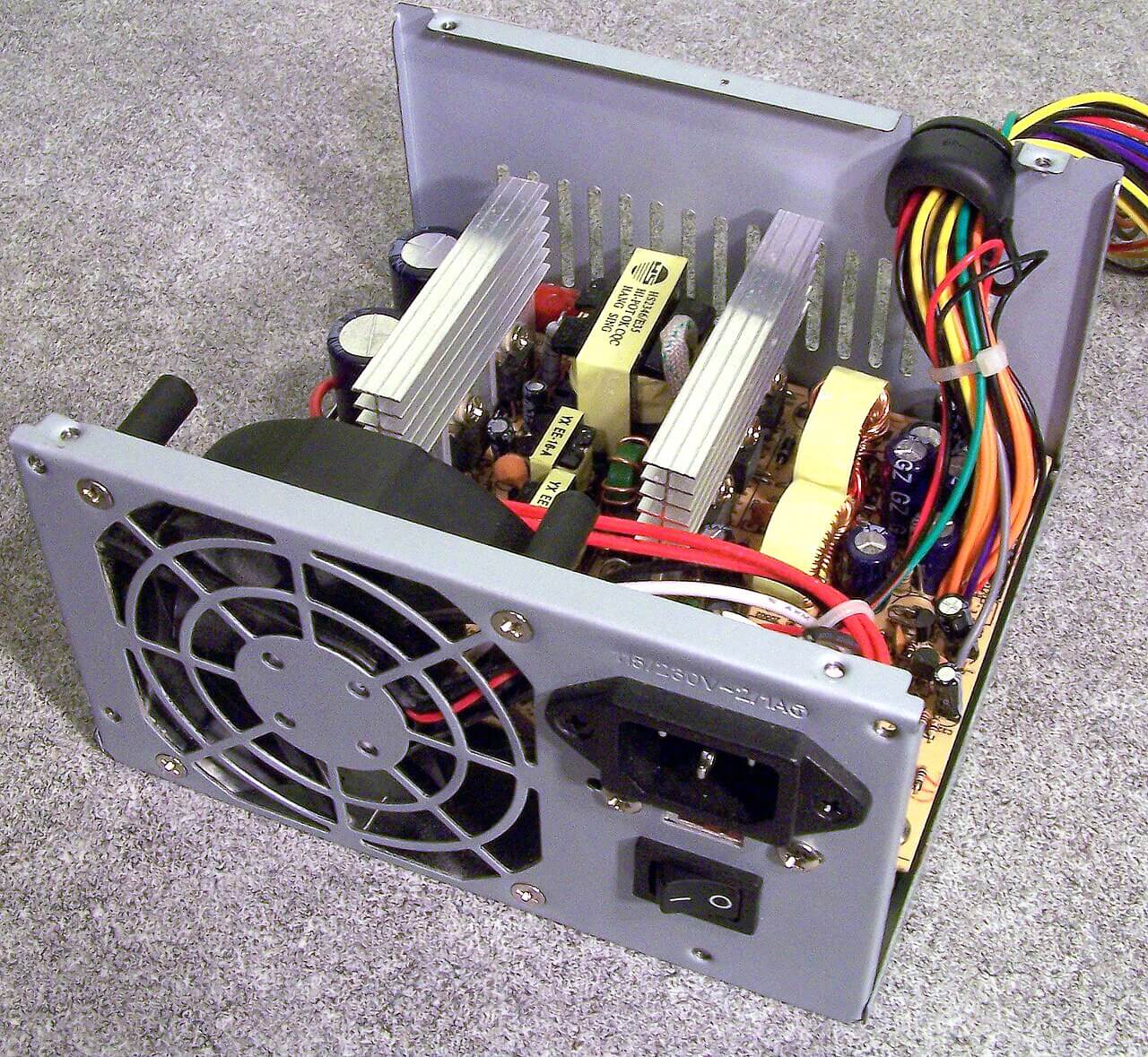
Power-supply and power-conversion boards frequently use THT for large transformers, large capacitors, relays, fuses, and power connectors. Wave soldering is best suited for repeated exposed joints, while selective soldering is more effective for localized areas with high thermal mass. Elements that need to be monitored include polarity, seating, barrel fill, lead clearance, creepage, and residue condition. Functional testing under defined input and load conditions verifies stable power delivery and identifies joints that may overheat during extended use.
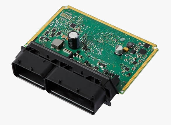
Automotive Control Modules
Automotive control boards usually contain SMT control circuits combined with THT connectors, relays, terminals, and large capacitors. Selective soldering protects neighboring SMT components from unnecessary heat. Close monitoring is required for connector alignment, lead support, barrel fill, keep-out areas, and vibration paths. Visual inspection, continuity testing, and functional testing should reflect the module’s expected outputs, thermal cycling, and vibration conditions rather than relying only on general acceptance criteria.
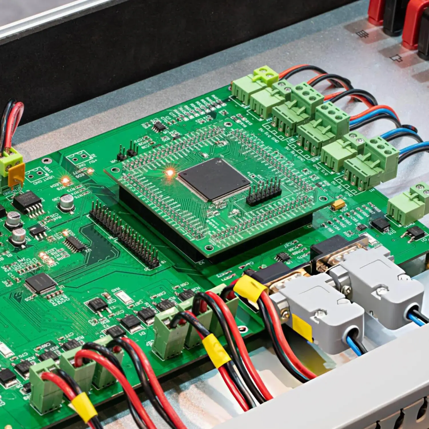
Industrial Control Systems
PLC I/O boards, motor-control interfaces, and field-terminal boards often use THT terminal blocks, relays, transformers, fuses, and power connectors. Mixed assembly provides density for control circuits while also providing additional support for field wiring. Important controls for THT include terminal alignment, barrel integrity, electrical spacing, and solder accessibility. Testing criteria may include continuity testing, relay activation, I/O response, and defined outputs. The mechanical characteristics of terminal joints should allow them to tolerate the specified wiring and tightening forces.
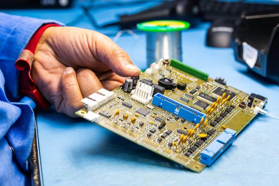
Medical Electronics
Medical control boards, sensor-interface boards, and device power-supply boards often use THT connectors, switches, relays, and large capacitors in combination with dense SMT circuits. When selecting a soldering technique for these medical devices, the layout and thermal sensitivity determine the use of wave or selective soldering. Key controls for THT use in medical electronics include polarity, seating, cleanliness, residue condition, and traceability of inspection results. Functional and electrical testing confirms that the assembly responds according to the specifications, while cleanliness requirements should match the enclosure, operating environment, and expected service life.
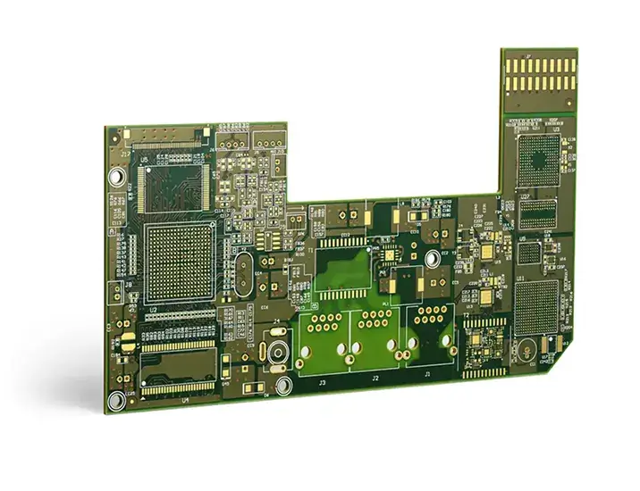
Aerospace and Defense Systems
Aerospace and defense electronic assemblies may use locking connectors, power terminals, relays, transformers, or other high-mass components as THT. The use of SMT logic with wave soldering, selective soldering, or controlled hand soldering is determined by board geometry and workmanship standards. Defined acceptance criteria should be established for lead support, connector retention, barrel fill, and thermal exposure. In addition, the shock and vibration performance of assemblies should be verified separately. When required, SUGA applies IPC-A-610J Class 3 workmanship to aerospace and defense electronic assemblies.
Consumer Electronics
Audio equipment, appliance controllers, power-input boards, and user-interface PCBs typically use THT for sockets, jacks, switches, relays, capacitors, and frequently operated connectors. SMT supports the remaining densely populated components. Wave soldering is suitable for accessible repeated joints, whereas selective soldering protects localized mixed-layout areas on boards. Common inspection items for these applications include alignment, bridging, lead protrusion, solder accessibility, and repeated-use forces. Connector and switch cycle-life testing should be based on the expected frequency of user operation.
What Can SUGA Assemble?
| Production Area | SUGA Deliverable Range | Assembly Impact |
|---|---|---|
| Board layer range | Up to 40 layers | Supports THT and mixed assembly on complex multilayer PCBs with plated component holes and controlled solder access |
| Copper range | Up to 1000 μm copper | Supports high-current and heavy-copper boards with controlled preheat and barrel filling |
| Component insertion range | Axial, radial, connectors, relays, transformers, terminals and large capacitors | Covers mixed mechanical, power and serviceable component requirements |
| Wave solder capacity | 8 wave soldering lines | Supports high-volume boards with exposed THT joint populations |
| Selective solder capacity | 4 selective soldering lines | Supports localized THT soldering on mixed assemblies near SMT features |
| Soldering method range | Wave, selective and controlled hand soldering | Matches underside exposure, geometry, volume and repair requirements |
| Production scale | Tens of thousands of boards per day | Supports high-volume THT and mixed-assembly production |
| Testing coverage | 100% visual inspection of accessible THT joints, plus AOI, X-ray, ICT and FCT | Covers visible geometry, internal solder distribution, electrical faults and defined board behavior |
| Prototype-to-volume support | Prototype iteration, low-volume builds and repeat production | Maintains consistent workmanship controls from prototype through volume production |
Through-Hole Assembly Constraints
The hole structure, internal connections, finished-hole design, and soldering access of multilayer assemblies are all affected by the addition of multiple layers. Heavy-copper designs, broad plane configurations, and high-thermal-mass leads create greater heat requirements for solder joints than standard assemblies. The component geometry determines whether automatic insertion systems are feasible or whether hand placement is required. The component geometry will dictate how the component should be retained without obstructing solder flow during the soldering process.
The number of layers and copper thickness are considered separately for each PCB build. The final construction of custom through hole PCBs is based on the materials used to manufacture the PCB, the manner in which copper is distributed in the PCB, the hole structure, the total board thickness, the clearance of each hole, and the heat required to solder the assembly.
Prototype To Volume Production
The available equipment used to manufacture PCB assemblies includes component preparation equipment, compatible automatic insertion systems, manual insertion workstations, wave soldering systems, selective soldering systems, controlled hand-soldering stations, lead-processing equipment, and inspection equipment. The criteria used to determine equipment selection include PCB geometry, component mix, production volume, workmanship class, whether a pallet or masking system is required, selective cycle time, manual intervention, inspection, and testing criteria.
The first production runs are often performed using controlled hand or selective soldering techniques to determine how well the components fit, whether they are placed with the correct polarity, whether soldering access is acceptable, whether the joints are formed properly, and what test coverage is available. Repeat production runs use compatible boards with wave soldering, selective soldering, or mixed soldering methods under consistent work instructions, programs, assembly fixtures, workmanship limits, and test conditions.
Our PCBA Production Lines
















Through-Hole Assembly FAQs
There is no fixed cost difference between through-hole assembly and SMT. Automated insertion and wave soldering can keep repeat THT production cost-competitive with SMT, while manual insertion, selective soldering, and additional inspection or rework increase the per-board cost as component count and process complexity increase.
Lead time for through-hole assemblies is driven more by component availability and process mix than by board size. While lead time for repeat assemblies using automatic insertion and wave soldering may decrease, lead time for assemblies using manual insertion, selective soldering, complex geometry, or extensive testing will increase.
Through-hole assembly processes are compatible with lead-free solder when compatible solder alloys, fluxes, component finishes, PCB surface finishes, and thermal profiles are used. During production of through-hole assemblies, the preheat, solder contact, and inspection requirements of each assembled PCB depend on the heat demand and wetting behavior of that particular PCB.
The finished hole size is determined by the maximum lead diameter, finished-hole tolerance, plating, component tolerance, insertion clearance, and solder-flow requirements. The finished hole size is specified by the component drawing and project design rules.
The main consideration when choosing between wave soldering and selective soldering is what is installed on the solder side of the PCB. Wave soldering is used for PCBs where most THT connections are in an open solder area. Selective soldering is necessary when nearby SMT features need to be protected from solder contact and requires a longer production cycle per PCB than a single wave-soldering pass.
A PCB can have both SMT and THT components installed. The critical factor is the order of assembly: SMT components are normally installed and soldered first so that THT components can be inserted afterward, avoiding unnecessary heat exposure for finished SMT solder joints. The order may change if a THT component’s height or shape prevents SMT placement or rework access. This must be resolved before production and is not a soldering-process default.
Acceptance criteria for THT solder joints are defined by IPC-A-610J under Class 1, 2, and 3 workmanship. The materials and processes used to produce THT solder joints are covered by IPC J-STD-001J. IPC-7711/21D applies when a solder joint requires rework or repair after inspection.