Upload BOM & Gerber
-
Mobile: +86 13312967631
-
Email: sales@sugaintl.com

SMT PCB Assembly Services
SMT Circuit Board Assembly Supplier in China — From Prototype Assembly to Volume Production
SUGA connects all the different stages in the production, inspection, and testing processes of SMT PCB assembly. Due to the multiple types and applications of SMT PCBs, engineers configure the SMT assembly steps for each PCB’s package type, production volume, component quality requirements, and package mix. From the first article to the final shipment of a PCB assembly, each order is tracked through all approved files, material lots, and inspection and test records.
18 SMT Lines.
Process-validated ±30 μm at 3σ, 0201 metric-class placement (0.25 × 0.125 mm), and double-sided 0.20 mm BGA assembly.
What Is SMT PCB Assembly?
SMT PCB assembly consists of placing components directly onto PCB pads using solder paste printing, automated placement machines, and controlled reflow processes. SMT and SMD refer to different parts of PCB assembly: SMT is the manufacturing method, and SMD refers to the component mounted using that method. PCBA describes the board after component assembly. Depending on the pitch, termination style, thermal mass, and inspection access, it may or may not be possible to place and inspect a component on a particular SMT assembly line.
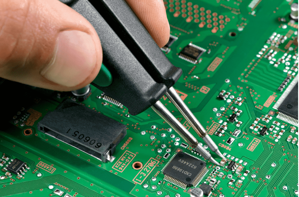
Surface Mount Devices
SMDs can include chip resistors, chip capacitors, SOPs, QFPs, QFNs, BGAs, and LGAs. For example, gull-wing leads are visible after the reflow process, whereas the solder joints for BGAs and LGAs are not directly visible after reflow. The component’s size and weight might fit within the placement machine but may require an alternate stencil aperture and a thermal profile specific to the PCB.
Package labeling is only an initial reference point. Engineers also need to verify the package’s body dimensions, lead or ball pitch, land pattern, moisture sensitivity, height, thermal limits, and the inspection method available to inspect the final solder joint.
SMT Assembly Trade-Offs
The ability to place a high number of devices quickly (high throughput) using small component sizes and assembly on both sides of the PCB, in addition to achieving a higher density of control electronics, is possible due to SMT assembly methods. Automated printing and placement processes provide more consistent production repeatability than manual insertion methods. Utilizing shorter interconnection paths can help make digital and communication product designs more compact; however, the actual electrical performance will still be determined by the stackup and layout of the PCB.
Rework on fine-pitch parts requires controlled heating and additional clearance around the target package.
While SMT provides many advantages for compact products, repeatable high-volume production, and fine-pitch devices, not all leaded devices will be replaced by SMT. Ultimately, reliability is determined by the combination of land pattern, materials used, board support, thermal design, process documentation, acceptance class, and operating environment.
SMT Assembly Process
The steps for the SMT assembly process move through verification of materials and data, preparing the board, printing solder paste, SPI, placing parts, reflow, inspecting, testing, and first-article verification.
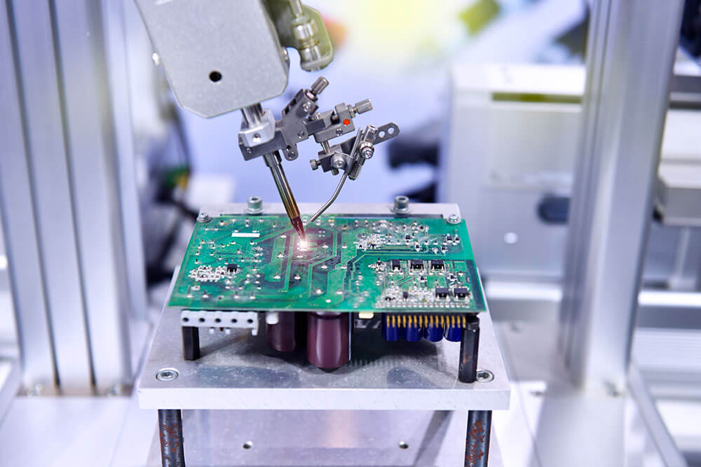
Pre-Print Verification
The first verification step is to ensure that the materials, BOM, Gerber or ODB++ files, centroid file, assembly drawing, polarity information, approved alternates, and test requirements all match the board revision being manufactured. Checks for material identification, quantity, lot information, packaging, and moisture sensitivity are also performed. Prior to loading the program, the operator verifies panel support and visible fiducials on the assembly.
These verifications help to decrease revision and setup errors. Verification of the materials, program revision, and feeder setup must occur prior to solder paste printing.
Solder Paste Printing
A stencil allows the application of solder paste to pads. The thickness and aperture geometry of the stencil, how it is aligned over the board, the amount of squeegee force applied, the speed of the printing process, the required separation, the condition of the paste, and under-stencil cleaning all affect the transfer of solder paste from the stencil to the PCB. The design range for stencil thickness is generally 4–8 mils, about 0.10–0.20 mm; this is a design range based on product technology. Different aperture designs or step stencils may be used for fine-pitch packages or large thermal pads.
IPC-7525C is the reference document for establishing stencil designs.
High-Speed Placement
The high-speed placement equipment picks parts from either a feeder or a tray and identifies each part using a vision system; it then places the part according to the centroid coordinates. Nozzle selection, polarity, fiducials or reference points, placement force, feeder setup, and line balance affect the results. The theoretical CPH for a placement machine will not be the actual CPH when processing a mixed product because of processing delays caused by package changes, board handling, inspection, and changeover times.
The first assembly board checks the revised program, part identity, part orientation, and how well the equipment has placed the parts. Using an AOI system or visual inspection, the assembler can examine visible features before proceeding with the production assembly run.
How Is Reflow Profiled?
The reflow process consists of five stages: preheat, soak, time above liquidus, peak temperature, and cooling to create a solidified bond. Preheating raises the temperature of the PCB without creating thermal shock. Soaking equalizes the temperature differences among the materials used in the assembly and activates the flux. Time above liquidus creates the solder connections. Peak temperature completes the wetting process. Cooling creates a solid bond at a controlled rate.
For SAC305, time above liquidus is commonly measured from about 217°C, and the peak of the profile is based on component limits, solder paste data, the thermal mass of the board, the distribution of copper, BGA or QFN construction, and repeated exposure during double-sided assembly. The oven setpoint alone does not provide as much process data as a thermocoupled board profile and its recipe revision provide together.
IPC/JEDEC J-STD-020F discusses the moisture and reflow sensitivity of non-hermetic SMDs. IPC/JEDEC J-STD-033D covers the storage, floor exposure, and handling of moisture-sensitive devices.
Post-Reflow Cleaning
Cleaning depends on flux chemistry, customer cleanliness requirements, conformal coating, high-impedance circuitry, contamination risk, and access beneath components. “No-clean” does not mean residue is acceptable under every coating or electrical condition. Conversely, washing a board does not automatically prove ionic cleanliness or coating adhesion.
After any required cleaning, the board goes through post-reflow inspection and testing. Post-reflow inspection and testing include checking visible joints, hidden joints, electrical connections, and powered functions using methods that reflect the board’s test risks and package configuration.
SMT Line Capacity and Board Range
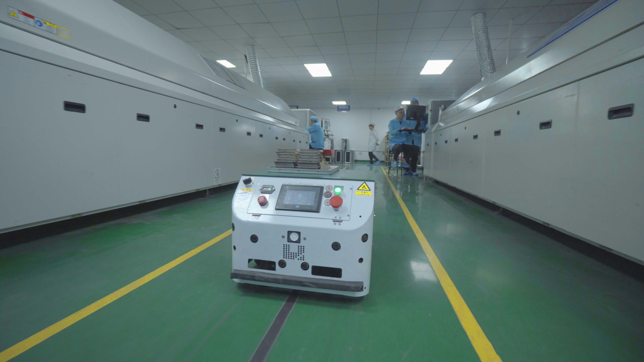
SUGA currently has 18 SMT lines matched to particular jobs based on package mix, pitch requirement, and board format.
Placement Platforms Across 18 SMT Lines
Across its 18 SMT lines, SUGA uses JUKI RS-1R, Yamaha YSM20R, and Panasonic NPM-W2 placement platforms. The JUKI RS-1R has an optimum speed of 47,000 CPH and a speed of 31,000 CPH under IPC-9850 conditions. The Yamaha YSM20R has a maximum speed rating of 95,000 CPH with two HM heads, while the Panasonic NPM-W2 has a maximum speed rating of 77,000 CPH with a 16-nozzle configuration.
SUGA’s SMT production lines handle PCB formats from 50 × 50 mm to large PCB formats up to 810 × 490 mm or 750 × 550 mm. They place components ranging from 0201 metric-class devices (0.25 × 0.125 mm) to 120 × 90 mm packages, long connectors up to 150 mm, and component heights up to 25 mm. The machine specifications of SUGA’s SMT equipment range from ±35 μm to ±25 μm under the stated conditions, with SUGA’s process-validated line accuracy achieving ±30 μm at 3σ. Actual placement rates depend on package mix, feeder changes, board movement, inspection loads, and line arrangement. SUGA maintains stable line output up to 60,000 CPH under typical production conditions.
| Engineering parameter | SUGA production range | Process dependencies | Control record |
|---|---|---|---|
| SMT production lines | 18 complete lines | board format, package mix and production volume | line allocation and lot records |
| Placement output | Stable output up to 60,000 CPH under typical line configurations | package mix, feeder changes, board handling and inspection load | production plan |
| Placement accuracy | Process-validated full-line accuracy down to ±30 μm at 3σ | package pitch, land pattern, fiducials and paste transfer | process capability data |
| Small components | 0201 metric-class support (0.25 × 0.125 mm) | pad design, stencil aperture, solder-mask registration and AOI resolution | print, placement and inspection results |
| Fine-pitch BGA | 0.20 mm ball pitch for selected projects | pad geometry, via strategy, paste deposit, warpage and X-ray coverage | DFM, profile and X-ray results |
| Double-sided assembly | Double-sided SMT and fine-pitch BGA supported | first/second-side sequence, component mass, repeated thermal exposure and support | process sequence and inspection records |
| Stencil thickness | Regular 4–8 mil range | package geometry, paste transfer and thermal-pad requirements | stencil specification and SPI results |
| Mixed technology | Supported | connector load, high-current parts, selective/wave solder compatibility and thermal mass | assembly sequence and post-solder inspection |
| Production stage | Prototype through volume production | setup reuse, controlled alternates and test capacity | build and test records |
Integrated SMT Line Configuration
The setup for standard SMT assembly includes the printer, SPI, pick-and-place equipment, reflow oven, and AOI systems. Additional tests that could follow in the manufacturing line are X-ray inspection, electrical testing, and functional testing, which will vary with the type of product and package used.
Fine-Pitch Placement
Fine-pitch work combines placement accuracy with paste transfer and inspection. Dense layouts are still dependent upon land patterns, solder-mask registration, warpage control, and stencil design for each package. Package-specific pad, solder-mask, stencil, reflow, and X-ray controls are used for selected BGA assemblies with 0.20 mm ball pitch.
Fiducial marks are available in a large range of sizes, including Ø1–3 mm; common sizes are Ø1.0–1.5 mm. The final mark size and clearance are dependent on the machine used, available board space, and design specifications.
Double-Sided Assembly
Double-sided SMT assembly requires a deliberate sequence for the first and second sides. The design engineer must determine how much mass is associated with the components on the second side, the geometry of the joints, the effect of repeated thermal exposure, and whether paste or adhesive is the most effective means of holding the components in place. The weight of the components on the second-reflow face will require adequate mechanical support, since gravity and repeated thermal exposure will both work against those joints.
The inspection process includes checking both sides of the PCB. The default method for inspecting hidden joints on double-sided BGA assemblies with 0.20 mm ball pitch is X-ray.
Prototype to Volume
The transition from prototype to volume production begins with the engineer learning from the prototype and first-article builds and retaining the BOM, programs, profiles, inspection coverage, and test baselines. The same items can be reused in subsequent lots, provided the design and materials remain unchanged. Higher output is one factor in volume production. Fixture capacity, controlled substitutes, inspection depth, traceability, and consistent test coverage will help determine whether the process can replicate the initial successful build.
Common SMT Assembly Defects
The majority of SMT assembly defects are the result of issues associated with paste transfer, component placement, component condition, pad design, solderability, and thermal behaviour. In diagnosing SMT assembly defects, it is essential to relate the visible or electrical symptom back to the process step that caused the defect. Product acceptance criteria define whether a defect is acceptable. A generic list of SMT defects cannot determine whether a particular defect is acceptable.
| Defect mode | Primary process drivers | Detection signal | Root-cause check | Process control |
|---|---|---|---|---|
| Solder bridges | excess paste, aperture design, placement offset, pad spacing or wetting behavior | SPI and AOI for visible locations | electrical test for unintended shorts | aperture, paste volume, alignment, pad and profile control |
| Open joints | insufficient paste, blocked aperture, poor solderability, non-coplanar leads or incomplete wetting | SPI plus AOI for visible joints | X-ray for hidden joints and electrical test for connection | stencil cleaning, solderability, coplanarity and thermal control |
| Solder balls | moisture, paste condition, contamination or poorly controlled heating | visual inspection or AOI | cleanliness evaluation only when contamination is the concern | MSL, paste handling, board cleanliness and profile control |
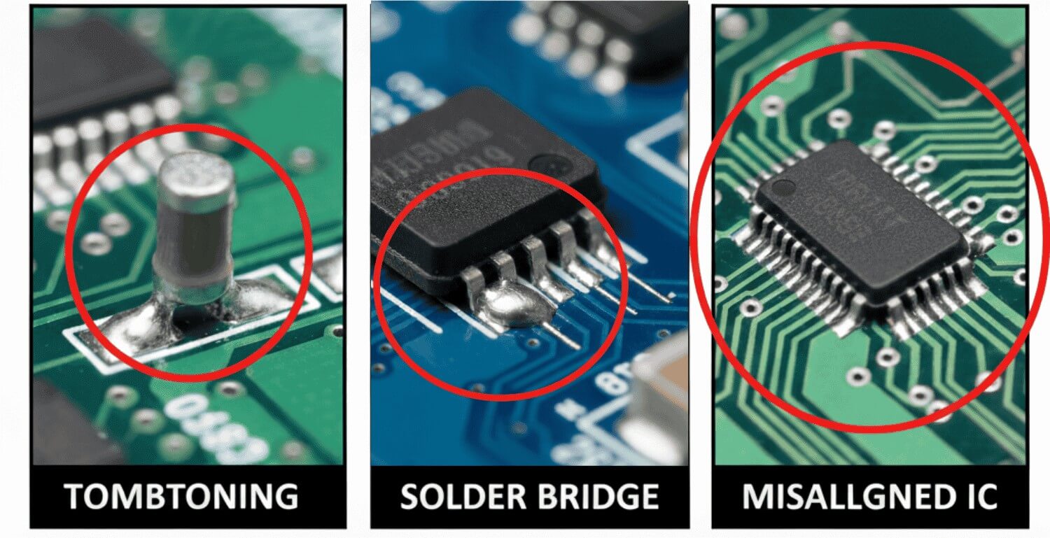
| Tombstoning | unequal wetting, asymmetric pads, copper imbalance or uneven deposits | AOI | process and pad analysis | pad symmetry, copper balance, paste and placement control |
| Component misalignment | fiducial, program, feeder, pickup, paste-registration or placement error | AOI | first-article findings and functional effect where relevant | data, vision, feeder and print controls |
| Solder voids | trapped volatiles, moisture, aperture pattern or limited gas escape | X-ray | thermal or electrical assessment | MSL, paste, aperture and profile optimization |
| Lifted leads | lead coplanarity, placement height, package damage or thermal stress | visual inspection or AOI | electrical test | incoming condition, placement and thermal controls |
| De-wetting / non-wetting | oxidation, contamination, poor finish, storage or flux mismatch | visual inspection or AOI for visible joints | solderability analysis when root cause is unclear | surface finish, storage, cleanliness and flux control |
| Skewed / rotated parts | centroid, pickup, nozzle, feeder or uneven deposit | AOI | first-article verification | data, nozzle, fiducial and print controls |
| Component damage | excess heat, moisture, mechanical force, ESD or handling | visual/AOI for external damage | electrical or functional test for latent or internal failure | MSL, ESD, nozzle force, handling and thermal limits |
Solder Bridges
Bridges formed repeatedly at the same package or aperture suggest that there is a systematic issue with printing, land-pattern geometry, or registration. Correlating SPI data with AOI location data helps to differentiate paste-volume drift from placement offset or differences in wetting.
Open Joints
For an open joint, the primary question is whether the connection was never made or failed as a result of coplanarity, solderability, or a lack of thermal energy. By comparing print data, component condition, images of hidden connections, and net test results, a reliable diagnosis can be made of where the failure occurred.
Tombstoning
Tombstoning is the lifting of one end of a small two-terminal component due to an imbalance in wetting forces. Off-center placement of the component and its thermal behaviour may exacerbate the pad and paste factors mentioned above. AOI will detect the lifted component, while the print and profiling data will help to identify whether the imbalance originated from pad design, paste application, component placement, or heating.
Solder Voids
Solder voids are formed when gas cannot escape from molten solder located under BGAs, QFN packages, and large thermal pads. The primary means of detecting solder voids is X-ray inspection. The acceptance of solder voids depends on the thermal and electrical function of the solder joint and does not use one universal void percentage for all joints.
Component Misalignment
Component misalignment patterns involving the same reference designator generally indicate a problem in one of the following areas: program, fiducial, feeder, nozzle, or print-registration control. However, isolated cases typically indicate a pickup or component-condition issue. Reflow self-alignment can correct misaligned components with small offsets. However, it cannot correct an error that is systematic to the setup process itself.
SMT Inspection and Testing
| Inspection / test | Process point | Detectable condition | Coverage limit | Control purpose |
|---|---|---|---|---|
| 3D SPI | after printing | insufficient or excess paste, deposit offset, area, height and volume variation | does not assess placement, reflow quality or electrical function | stops systematic print defects before components cover the pads |
| AOI | after placement and/or reflow | missing or rotated parts, polarity, offset, bridges, lifted leads and visible fillets | cannot inspect joints hidden beneath bottom-terminated packages | catches visible placement and solder defects before final testing |
| X-ray / AXI | after reflow | BGA, LGA and QFN joint structure, hidden bridges, opens and void evidence | does not test firmware, interfaces or powered board behavior | shows hidden solder conditions outside optical line of sight |
| Flying probe | after assembly | continuity, shorts, opens and accessible component-network checks | cannot reproduce full product behavior or high-volume takt | provides electrical coverage without a dedicated fixture |
| ICT | after assembly | repeatable in-circuit measurements through designed test points | cannot test functions outside fixture and test-point coverage | supports faster electrical verification in repeat production |
| FCT | final board test | defined power rails, interfaces, sensors and programmed functions | may not locate the physical defect without diagnostic coverage | confirms that the assembled board performs its specified board-level functions |
| FAI | first assembled unit or controlled change | part identity, polarity, placement, workmanship, programming and baseline results | cannot demonstrate long-run stability by itself | establishes the SMT build baseline for later lots |
SMT workmanship follows IPC-A-610J acceptance criteria and J-STD-001J soldering requirements.
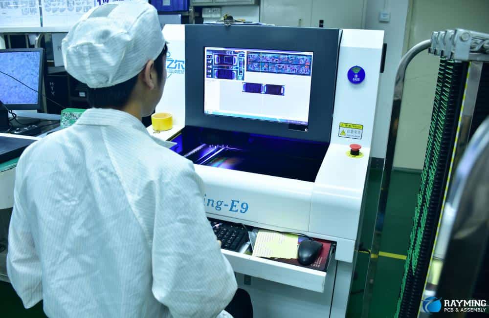
Solder Paste Inspection
SPI is especially beneficial for metric 0201, BGA/QFN, fine-pitch, and step-stencil work due to the small shifts in solder paste deposits on these types of assemblies. With SPI, trend data is used to help determine aperture adjustments, cleaning-frequency controls, and print-parameter corrections prior to further placement.
Automated Optical Inspection
The program coverage for AOI should be based on the visibility of the package, the amount of polarity risk, the lead geometry, and the acceptable level of false calls. In double-sided assemblies, camera access and shadowing will be assessed for each side individually.
X-Ray Inspection Triggers
The need for X-ray inspection is based on the type of part used, such as bottom-terminated packages, double-sided 0.2 mm BGA, thermal pads, suspected head-in-pillow, or voiding risk. Sampling or 100% inspection may be dictated by the risk associated with the package, historical lot information, or acceptance criteria.
Electrical / Functional Testing
Electrical and functional testing include two diagnostic layers. Keeping the two diagnostics separate will improve failure diagnosis and eliminate the need for functional testing to perform basic continuity tests.
First Article Inspection
FAI links the first accepted unit from production with the BOM, PCB revision, placement program, thermal profile, inspection settings, and test response. For later lots, the FAI will be used to identify changes in setups or materials and will not be used to create a new baseline for every build.
Board-Level SMT Results
Testing and inspection of SMT at the board level provide production information used to determine board-level assembly quality. SMT inspection and testing include visible inspection through AOI, X-ray inspection for hidden solder structures, FCT to verify defined powered functions, and FAI to provide the baseline for the first PCB build. Each inspection and testing method confirms a different aspect of board-level SMT assembly quality. However, complete qualification and certification of the finished product are performed at the system level.
SMT or Through-Hole Assembly?
SMT is ideal for compact, high-density, automated electronics. Through-hole assembly is selected for parts that need to be physically anchored more securely or cannot follow the SMT reflow process. Mixed assembly combines both assembly methods on the same board.
| Assembly demand | SMT response | Mixed-technology response | THT selection condition |
|---|---|---|---|
| Compact control and logic circuitry | Primary choice | Used when loaded parts share the board | Not normally the main choice |
| Fine-pitch ICs and dense passive networks | Primary choice | Combined with selected THT parts | THT does not replace fine-pitch SMT |
| Connectors with repeated insertion force | May require extra mechanical support | Common choice | Use when lead anchoring is required |
| Relays, transformers, large magnetics or odd-form devices | Possible only when package and reflow conditions allow | Common choice | Use when geometry, mass or heat prevents SMT processing |
| High-current or high-thermal-mass parts | Applicable to designed SMT power packages | Often preferred | Use when the component is intended for leaded mounting |
| Double-sided dense electronics | Primary choice | Possible with sequenced THT operations | THT selected only for specific components |
Mechanical Load Changes the Choice
Repeated connector insertion, board flex, vibration exposure, component weight, and strain relief will determine the mechanical load on the components. For example, a lead anchored through a plated hole may handle the force from an inserted connector better than a surface joint, but it is not necessarily the best choice in all environments. The choice also depends on board thickness, support, solder geometry, and actual loads.
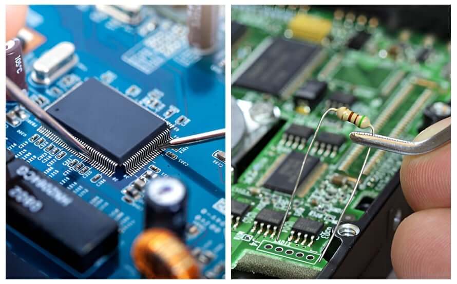
When Mixed Assembly Is Required
Mixed assembly typically consists of placing fine-pitch control electronics via SMT, followed by relays, transformers, loaded connectors, and leaded power components. The assembly process can use selective, wave, or manual soldering, depending on the geometry and thermal mass of the components. Other processes, such as cleaning, coating, post-THT inspection, handling, and testing, add costs to mixed assembly but do not change why the component requires mechanical or thermal accommodation.
What Drives SMT Assembly Cost?
Board area alone is a poor cost proxy.
| Manufacturing variable | Added process content | Cost effect |
|---|---|---|
| Placement count | feeder occupancy, placement time and inspection volume | higher recurring machine time per board |
| Package mix | nozzle and feeder changes, fine-pitch controls, MSL handling and package-specific inspection | higher setup and inspection content |
| Side count | a second print/place/reflow cycle plus additional board handling | higher setup, cycle time and inspection coverage |
| Stencil and setup | stencil, programs, feeder loading, profile, first article and test preparation | non-recurring cost amortized over lot size |
| Inspection depth | SPI, X-ray, electrical fixtures, FCT programming and test takt | cost rises with coverage, fixture content and test time |
| Material condition | partial reels, trays, moisture controls and customer-supplied kits | more receiving, kitting and line-preparation time |
| Mixed technology | THT insertion, selective/wave/manual soldering and post-solder inspection | additional operations beyond SMT placement |
| Production volume | setup reuse and longer uninterrupted production runs | lower setup cost per unit when the build remains stable |
| Yield and rework exposure | warpage, poor paste transfer, difficult packages and limited test-point coverage | higher engineering, diagnosis and recovery cost |
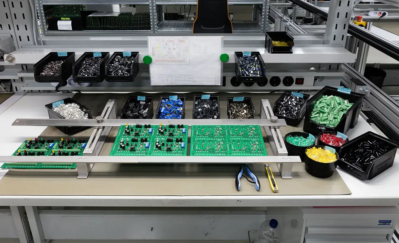
Setup Cost Drivers
Setup cost is front-loaded. Subsequent orders provide an opportunity to reuse the assembly stencil, programs, and test setup if they remain applicable to the current revision.
Package Mix Cost
Package density affects assembly cost because of the process-window and diagnostic burden, not just because of board size. A compact, high-density board may require more engineering and inspection than a physically larger board with less dense and simpler content.
How Does Volume Change Cost?
Volume decreases unit cost when the programs, fixtures, material conditions, and line balance are reusable. Volume does not eliminate the need for first-article inspection or test coverage; however, it spreads the fixed costs over a greater number of assemblies and increases the cost of an uncontrolled change.
SMT Assembly Applications
SMT PCB assembly is used for highly compact and repeatable electronics across consumer, communications, automotive, aerospace, medical, industrial, IoT, wearable, and energy applications when process controls are matched to each type of PCB.
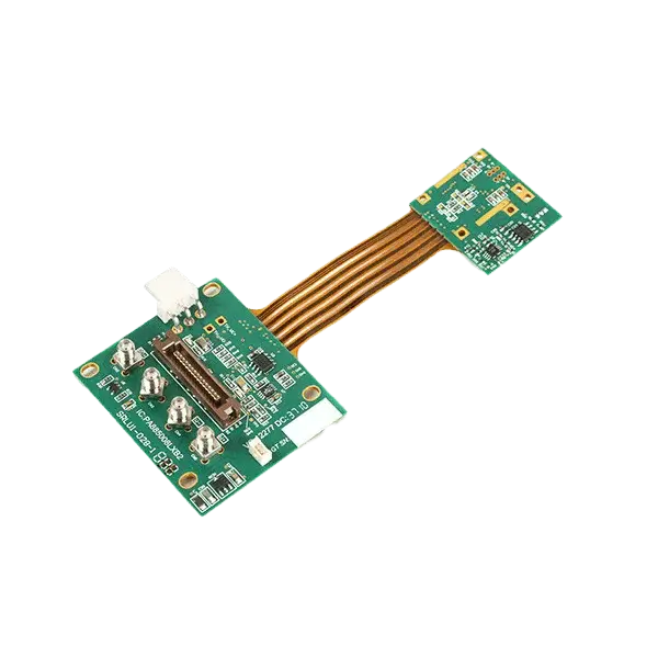
Consumer / Mobile Electronics PCB
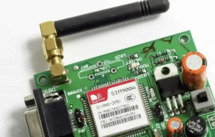
Consumer and mobile PCBs use processors, memory, power management systems, wireless modules, fine-pitch ICs, dense passive components, and compact connectors. Creating PCBs with small spacing and double-sided placement increases the importance of stable paste transfer, metric 0201 placement, second-side sequencing, and hidden-joint inspection for bottom-terminated packages.
Telecommunications PCB
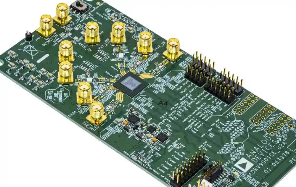
Telecommunications PCB designs commonly use BGA or QFN controllers, dense passive networks, power rails, high-speed interfaces, and communication modules. A fine-pitch communication control PCB will require careful stencil design, a measured reflow profile, firm PCB support, and an inspection system matched to visible and hidden solder joints.
Automotive Electronics PCB
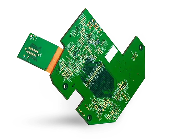
Automotive PCBs include control modules that connect sensors, power management, communications, and loaded connectors. Automotive connector and relay joints experience vibration-driven solder fatigue, while under-hood thermal cycling stresses BGA and lead-free joints. SUGA applies IATF 16949:2016 controls to automotive SMT assembly.
Aerospace / Defense PCB
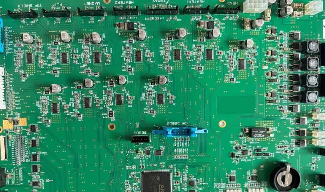
Control, navigation, communication, power-conditioning, and sensing PCBs may require very tight control of board configuration and traceability. Pure-tin or high-tin component finishes require tin-whisker risk assessment for long-life aerospace and defense applications. Launch and flight vibrations create additional mechanical stress on hidden BGA joints, requiring appropriate qualification and X-ray inspection. SUGA applies AS9100D controls to aerospace and defense SMT assembly.
Medical Device PCB
Medical electronic products include a combination of sensor interfaces, control circuits, power management systems, displays, and communication features. Implantable boards carry a higher cleanliness and biocompatibility burden than wearables. PCBA lot records should support linkage to the finished device’s serial number, device history record, and unique device identifier traceability system. SUGA applies ISO 13485:2016 controls to medical electronics assembly.
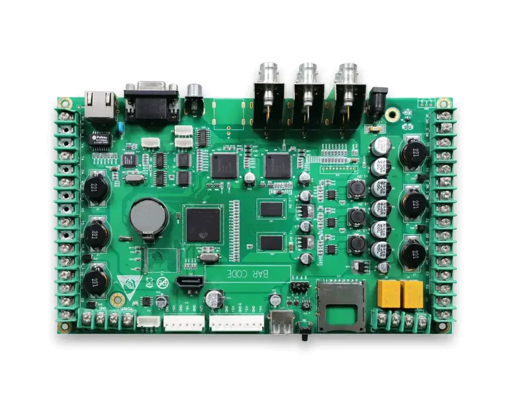
Industrial Automation PCB
Industrial automation controllers usually combine programmable logic controller inputs and outputs, motor-control logic, sensor interfaces, communications, relays, terminals, and power sections. An industrial automation controller may use SMT for dense control circuitry, followed by selective, wave, or manual through-hole soldering for loaded components. Inspection and testing of the industrial controller will cover both the reflowed SMT section and the later soldering operation.
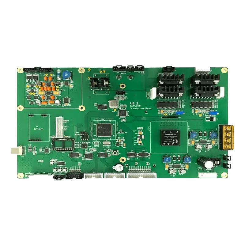
IoT Sensor PCB
An IoT sensor PCB may place the wireless module and MCU on one side while placing compact passive components and sensor circuitry on the opposite side. Many factors affect the SMT assembly sequence, such as component mass, two reflow cycles, moisture-sensitive components, PCB support during assembly, programming, and proximity to the battery. Both sides of the PCB should be inspected. Where a component hides the solder joint, X-ray inspection should be used.
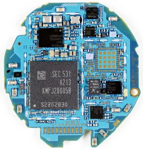
Wearable Electronics PCB
Wearable electronics PCBs consist of thin rigid, flex, or rigid-flex sections combined with sensors, radios, battery interfaces, and compact connectors. Factors to consider when designing a PCB for wearable electronics applications include fine-pitch component requirements, flex handling, warpage, restricted clearance, and rework access. These factors require appropriate support, restrained thermal exposure, and suitable inspection access based on the component layout.
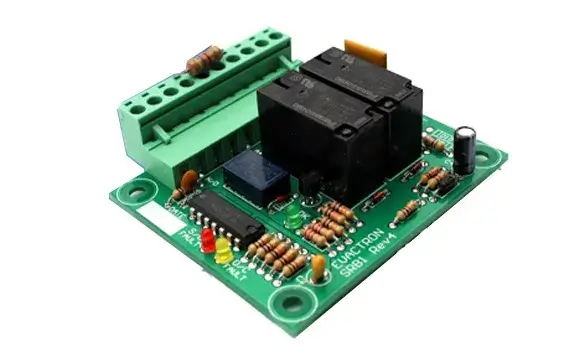
Energy / Power Electronics PCB
Energy and power electronics PCBs are assemblies of control and metering equipment, driver circuits, isolated interfaces, terminal connections, magnetics, power devices, and thermal pads. When designing a PCB for energy and power applications, large thermal mass, high-current paths, voiding in solder connections, and creepage or clearance restrictions can result in mixed assembly. The control or driver circuits can use SMT, while terminals or leaded power devices may require mechanical anchoring and a separate solder operation. A hidden thermal-pad solder joint may require X-ray inspection.
Choosing an SMT Assembly Supplier
SUGA provides SMT PCB assembly in Shenzhen and the Pearl River Delta, with board-specific engineering, inspection, testing, and traceability for SMT PCB assemblies. Selecting a supplier starts with matching the PCB format, component range, pitch, side count, warpage support, and estimated output to the actual configuration of the SMT line.
The inspection plan should define whether SPI, AOI, X-ray, electrical testing, FCT, or FAI will be used. Visible-joint, hidden-joint, test-point, and functional risks should be assigned to the appropriate inspection or testing method. A machine list without board mapping, or one inspection method presented as complete coverage, does not show how the assembly will be controlled.
Traceability Controls
Traceability links the BOM and PCB revision to material lots, placement programs, thermal profiles, inspection records, test results, and shipped-lot identifiers. Testing and inspection records remain associated with the exact boards shipped.
Changes to an approved alternate component, stencil, program, or manufacturing site that affect the lot must be documented so that they remain traceable to the affected shipment lot.
Repeat Production Support
Repeat production depends on reusable placement programs, thermal profiles, fixtures, first-article criteria, and testing strategy. All approved alternate components and production-process changes must be evaluated before being introduced into a repeat order to ensure that later lots reproduce the accepted build.
Prototype speed may be less important when material substitutions, process settings, or manufacturing locations can change without corresponding production records.
Engineering Response
The engineering response to the submitted boards includes land-pattern evaluation, stencil-aperture evaluation, thermal evaluation, board-support evaluation, package-visibility evaluation, test-point coverage, and likely defect modes. A useful response links each risk to a defined action—for example, linking a bottom-terminated package to a stated X-ray sampling rate rather than a general inspection claim.
Our PCBA Production Lines
















Frequently Asked Questions
Most SMT components can be removed and replaced, but feasibility depends on package size, pad condition, available space around the component, thermal sensitivity, board construction, and access for controlled heating and inspection. BGA or QFN rework may require X-ray inspection and reliable profile control. Repeated thermal cycles can increase exposure for pads, laminate materials, and surrounding components.
High-load connectors, large odd-form components, some magnetics, leaded power devices, and components that cannot tolerate the selected reflow sequence may require through-hole mounting, selective soldering, manual procedures, or special support. The manufacturing process used for a specific component depends on its construction, mechanical load, thermal constraints, and the end-product design. High power alone does not automatically require THT.
A quote for SMT assembly typically requires the BOM, Gerber or ODB++ data, centroid or pick-and-place file, assembly drawing, order quantity, and any programming, inspection, or testing requirements. Approved alternates, panel data, and polarity information help confirm the setup and material requirements.
Yes. Double-sided SMT assembly requires a controlled first-side and second-side assembly sequence. Before the second reflow, an engineer must confirm the mass of the components on the second side, understand the joint geometry, confirm the proper board support, evaluate repeated thermal exposure, and confirm inspection access. Hidden joints on either side may require X-ray inspection.
SUGA supports 0201 metric-class components (0.25 × 0.125 mm). In addition to the metric 0201 component size, other factors that influence assembly success include pad geometry, solder-mask registration, stencil aperture, solder paste transfer, placement accuracy, PCB stability, and AOI resolution. Therefore, component size and the overall PCB design must be considered together.
BGA joints are hidden beneath the package; therefore, AOI cannot inspect these joints directly. X-ray inspection checks solder distribution, bridges, opens, void evidence, and other hidden structural conditions. Electrical or functional testing confirms connectivity or defined board behaviour. SUGA uses X-ray by default for 0.2 mm-pitch and double-sided 0.2 mm BGA assemblies.